

Overlay alignment measurement of wafers
a technology of alignment measurement and wafers, applied in semiconductor/solid-state device testing/measurement, semiconductor/solid-state device details, instruments, etc., can solve the problem of limited accuracy of prior ar
- Summary
- Abstract
- Description
- Claims
- Application Information
AI Technical Summary
Benefits of technology
Problems solved by technology
Method used
Image

Examples
Embodiment Construction
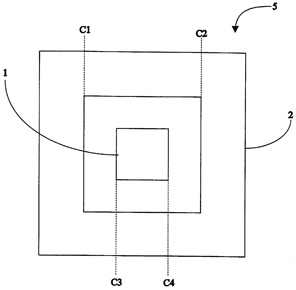
The present art of alignment measurement uses a "box in a box" type target 5 that is typically like the one illustrated in FIG. 1a. Inner box 1 is typically printed on the top layer of the semiconductor wafer being produced, while the open-center-outer block 2 is printed on the second layer down on the semiconductor wafer. The measurement process thus involves imaging of target 5 on an electronic camera, by means of a microscope system, at a high magnification (1000.times., typically) and with high resolution in both x and y directions.
The registration error in each of the x and y axes is measured by first calculating the locations of the edges of lines c1 and c2 of the outer box 2, and the edge locations of the lines c3 and c4 of the inner box 1. From those locations the misregistration between the two boxes is determined by comparing the average separation between lines c1 and c3 with the average separation between lines c4 and c2 (i.e., the misregistration between boxes 1 and 2 i...
PUM
 Abstract
Description
Claims
Application Information