Apparatus for spin coating, a method for spin coating and a method for manufacturing semiconductor device

Inactive Publication Date: 2000-03-07
FUJITSU SEMICON LTD
View PDF39 Cites 50 Cited by
  • Summary
  • Abstract
  • Description
  • Claims
  • Application Information

AI Technical Summary

Problems solved by technology

This is wasteful since the scattered resist cannot be reused.
Thus there is a problem that a patterned photoresist film formed by exposing and developing the photoresist film varies in a pattern size.
Further, there is also a problem that in an extreme case it is impossible to form a pattern of the photoresist film in the fringe part of the wafer 11 since an area uncovered with photoresist film 12 exi

Method used


Image

  • Apparatus for spin coating, a method for spin coating and a method for manufacturing semiconductor device
  • Apparatus for spin coating, a method for spin coating and a method for manufacturing semiconductor device
  • Apparatus for spin coating, a method for spin coating and a method for manufacturing semiconductor device

Examples


first example

(A) First example

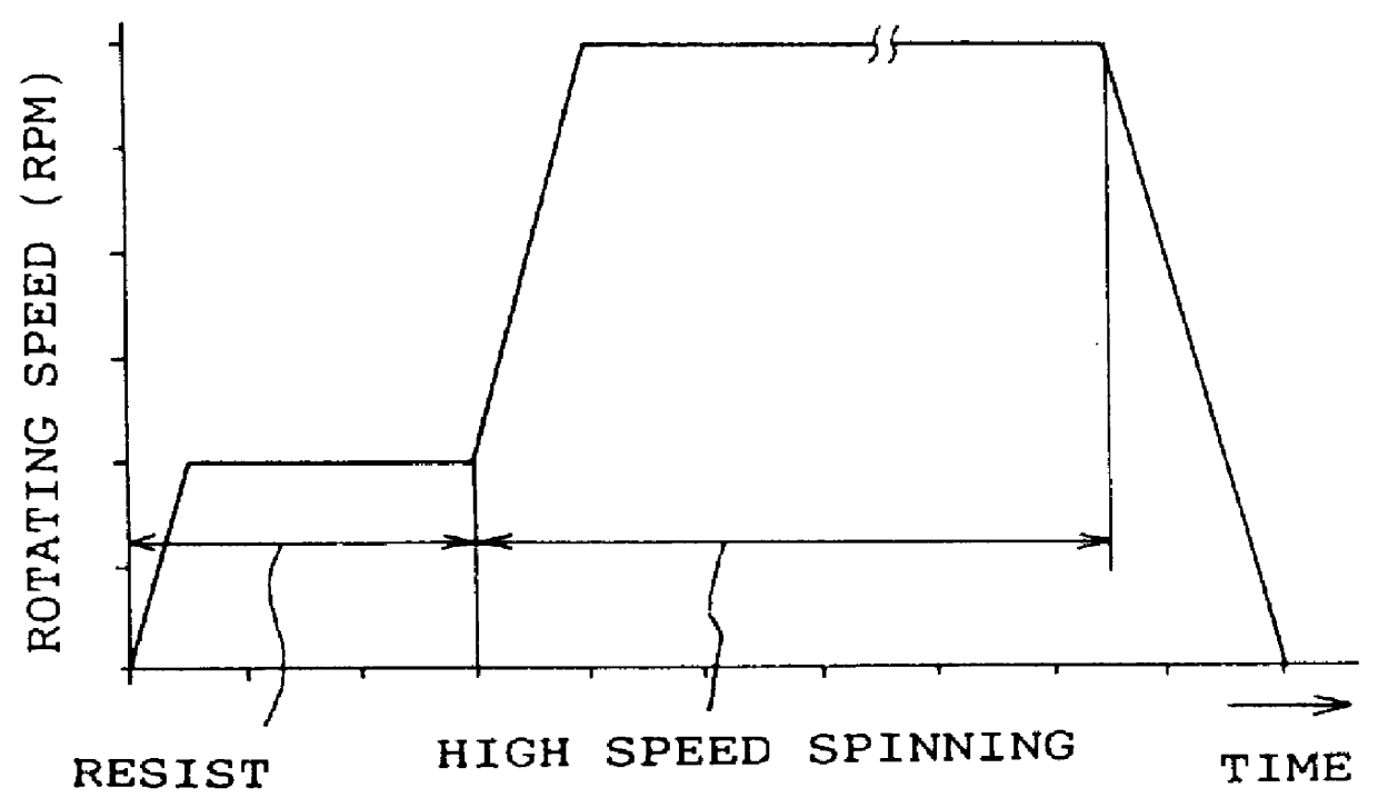
In a first example, three kinds of photoresist films are formed as using a solvent spreading period (t3) after dripping the solvent as a parameter. In order to examine variation in thickness of the photoresist films in relation to the solvent spreading period (t3) after dripping the solvent, the period (t3) is changed in such three stages as t3=0,4, and 5 seconds, where a condition of t3=0 shows that the process goes to the dripping period (t5) immediately after the solvent prespinning period (t2) without passing through the solvent spreading period (t3).

Each of FIGS. 6A to 6C shows an on-the-surface distribution of thickness of each of three kinds of photoresist films formed on the wafer 20 by means of the above-mentioned spin coating method. FIGS. 6A, 6B, and 6C show, respectively, the cases of t3=0 second, t3=4 seconds, and t3=5 seconds. In each of these cases, the axis of ordinates shows thickness (A) of a film and the axis of abscissas shows location in the waf...

second example

(B) Second example

In a second example, three kinds of photoresist films are formed as using an ambient temperature around the rotatable table as a parameter.

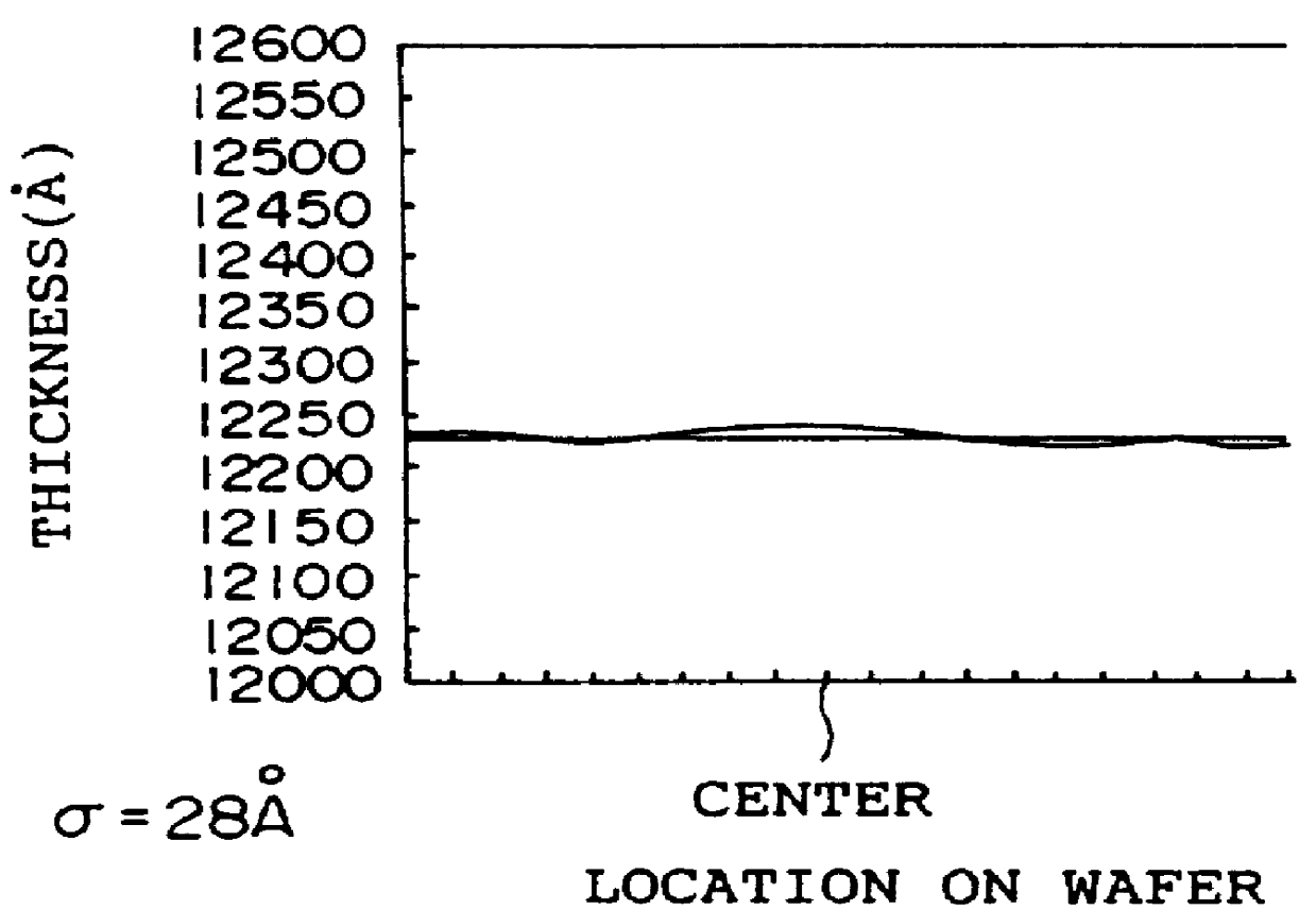
FIGS. 7A to 7C show thickness of photoresist films and variations in thickness of the resist films which were formed using the same method as mentioned above, as changing an ambient temperature (T) around the rotatable table in three stages of 21.degree. C., 23.degree. C., and 25.degree. C. and setting a solvent spreading period (t3) as 4 seconds.

FIGS. 7A, 7B, and 7C show, respectively, the cases of T=21.degree. C., T=23.degree. C., and T=25.degree. C. In each of these cases, the axis of ordinates shows thickness (A) of a film and the axis of abscissas shows location on the wafer.

In the embodiment, the following data were obtained.

1) In case of T=21.degree. C., Average film thickness=11750 .ANG..sigma.=62 .ANG.

2) In case of T=23.degree. C., Average film thickness=11800 .ANG..sigma.=44 .ANG.

3) In case of T=25.degree. C., Average ...

third example

(C) Third example

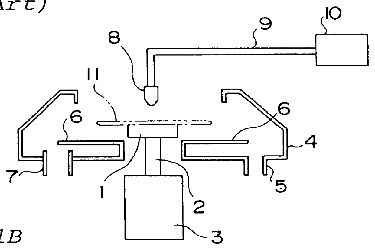
FIG. 9A is a side view showing a schematic structure of a spin coating apparatus according to a third embodiment of the invention. What distinguishes this apparatus from the spin coating apparatus according to the first example shown in FIG. 3 is the fact that both of a resist solution discharging means 28a and a solvent discharging means 29a are disposed above the center part of the surface of a wafer 20a and fixed in the location, namely, a resist solution and a solvent are supplied from the same location. As for symbols in FIG. 9A, a symbol having the same number as FIG. 3 shows a part equivalent to that in FIG. 3.

FIG. 9B is a timing chart showing a process sequence by a method for spin coating which uses the spin coating apparatus according to the third example.

Resist films were formed on the wafer 20a by means of the spin coating apparatus shown in FIG. 9A and according to the timing chart in FIG. 9B.

First, the wafer 20a is fixed on the rotatable table 21a by s...


PUM


Abstract

The invention relates to an apparatus for spin coating for forming a resist film, an SOG film, a polyimide film, and the like in manufacturing semiconductor devices and has the object of forming a coated film with a specified and uniform thickness even in case that an amount of discharged coating solution is a little. An apparatus for spin coating of the invention comprises a rotatable table for placing a wafer, a coating solution discharging means which is set above the rotatable table and discharges a coating solution on the surface of the wafer, and a solvent discharging means which is above the rotatable table and discharges a solvent capable of dissolving the coating solution.

Description

1. Field of the InventionThe present invention relates to an apparatus for spin coating and a method for spin coating, and more particularly to an apparatus for spin coating and a method for spin coating which are used for forming a resist film, an SOG (spin-on-glass) film, a polyimide film, and the like in manufacturing semiconductor devices.In manufacturing a semiconductor device, a photoresist film is formed as an etching resistant mask to be used in patterning an insulating film and a conductive film, and an SOG film is formed as an interlayer in a tri-layer resist system, and furthermore a polyimide film is formed as a covering insulating film.These various films are often formed by spin coating and it is desired for them to be made uniform in thickness. As for a photoresist film used as an etching resistant film and an SOG film as an interlayer in a tri-layer resist system, in particular, it is necessary to make them thin and uniform in thickness in case of forming a fine patt...

Claims


Application Information

Patent Timeline
IPC IPC(8): B05C11/08G03F7/16B05D1/40B05C5/00H01L21/027H01L21/312
CPCB05C11/08G03F7/162
Inventor KIKUCHI, KENJIMURAMATSU, TOMOAKI
Owner FUJITSU SEMICON LTD
Why Eureka
Try Eureka