Electroluminescent display device

a technology of electroluminescent display device and circuit, which is applied in the direction of electric digital data processing, instruments, computing, etc., can solve the problems of large power source circuitry, large drive power consumption per cycle, and large integration and cos

Inactive Publication Date: 2000-05-16
DENSO CORP
View PDF13 Cites 62 Cited by
  • Summary
  • Abstract
  • Description
  • Claims
  • Application Information

AI Technical Summary

Problems solved by technology

Because a general purpose driver IC does not have such a high breakdown voltage, it is necessary to specially design a high breakdown voltage driver IC which has a high breakdown voltage to satisfy the above requirements, and this causes problems in terms of integration and cost.
Further, when the rear electrode has been grounded and a positive and negative alternating current signal is applied to the transparent electrode, two types of positive and negative power sources normally become necessary, and power source circuitry becomes large.
Also, d

Method used


Image

  • Electroluminescent display device
  • Electroluminescent display device
  • Electroluminescent display device

Examples


first embodiment

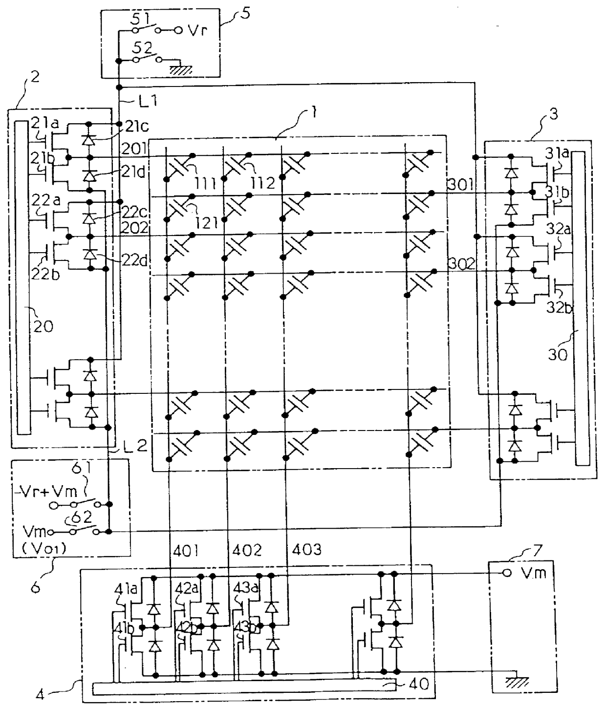
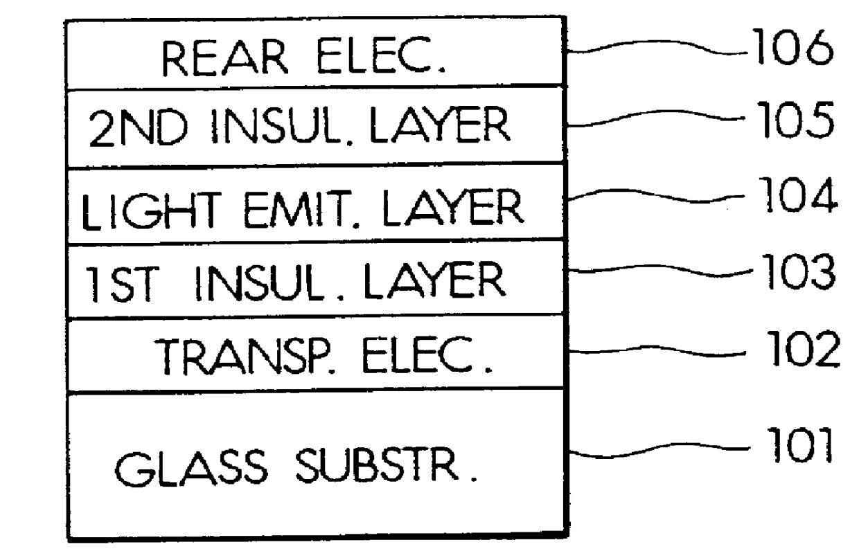
FIG. 1 shows an overall structure of an EL display device according to the present invention. In this Figure, an EL display panel 1 has a plurality of transparent electrodes and back electrodes in columns and rows as scan electrodes and data electrodes, and is structured to perform matrix display.

In specific terms, as shown in FIG. 1, odd-numbered scan electrodes 201, 202, 203, etc. and even-numbered scan electrodes 301, 302, etc. are formed along the column direction of the display, and data electrodes 401, 402, 403, etc. are formed along the row direction of the display 1.

EL elements 111, 112, etc. are formed as pixels at intersections of the scan electrodes 201, 301, 202, 302, etc. and the data electrodes 401, 402, 403, etc. The EL elements are capacitive elements and are represented by capacitor symbols in the Figure.

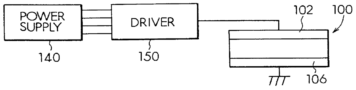
Scan side driver ICs 2 and 3 and a data side driver IC 4 are provided to perform display drive for this EL display panel 1.

The scan side driver IC 2 is a push-pull ...

second embodiment

Furthermore, according to this second embodiment, lowering of breakdown voltage with respect to both the scan side driver ICs 2 and 3 and the data side driver IC 4 was provided, but it is also acceptable to lower the breakdown voltage with respect to only the data side driver IC 4 if such is necessary.

Additionally, as shown in FIGS. 6A-6C, when 1 / 2 of modulation Vm is taken as the offset voltage V.sub.02, a differential voltage applied to the EL element during electroluminescence and during non-electroluminescence can be optimized.

According to the above-described embodiments, a device to perform matrix display where a plurality of scan electrodes and a plurality of data electrodes are mutually perpendicular was described, but this invention can be applied also in a device to perform segmented display. In this case, it is sufficient to perform control so that positive and negative drive voltage pulses are applied to each segment with respect to the device shown by the timing diagrams...


PUM


Abstract

A scan driver IC for an EL element in an EL display device supplies, in a positive field, a positive polarity scan voltage and an offset voltage which is higher than ground to scan side driver ICs from voltage supply circuits, and the scan side driver ICs set voltage of scan electrodes to be the offset voltage in the positive field, together with outputting the positive polarity scan voltage to the scan electrodes during electroluminescence timing. Consequently, a voltage of Vr-Vm is applied to the scan side driver ICs, and so the breakdown voltage can be lowered by an amount corresponding to the offset voltage Vm. Circuits for providing such voltages, for providing alternating current drive voltages, and for reducing power consumption of the drive circuits are also disclosed.

Description

1. Field of the InventionThis invention relates to a circuit for driving an electroluminescent (EL) display device.2. Description of Related ArtA device disclosed in Japanese Patent Application Laid-Open Publication No. Hei 5-333815 is known as a circuit for driving an EL display.According to this device, EL elements in the display are arranged in a matrix and a scan side driver IC and data side driver IC are respectively provided on a scan side and data side of the display elements. Accordingly, drive voltage pulses having a differing polarity with each positive and negative field are applied to the EL elements by the respective driver ICs and the EL elements emit light.That is to say, in the positive field, a ground voltage (0 V) is taken to be a reference voltage and a voltage Vr corresponding to an EL drive voltage is output to a scan electrode of the EL display from the scan side driver IC, and from the data side driver IC, the ground voltage is output to the EL element so that...

Claims


Application Information

Patent Timeline
IPC IPC(8): G09G3/30
CPCG09G3/30G09G2330/023G09G2310/0275G09G2310/0267
Inventor KISHITA, HIROYUKIOSADA, MASAHIKOHIMI, HIROAKI
Owner DENSO CORP
Why Eureka
Try Eureka