

In plane switching LCD with 3 electrode on bottom substrate and 1 on top substrate
a technology of liquid crystal electrooptical devices and bottom substrates, applied in non-linear optics, instruments, optics, etc., can solve the problems of certain limit of response speed in switching between states, unclear or unnatural display, and inability to increase the response speed of the devi
- Summary
- Abstract
- Description
- Claims
- Application Information
AI Technical Summary
Problems solved by technology
Method used
Image

Examples
first embodiment
[First Embodiment]
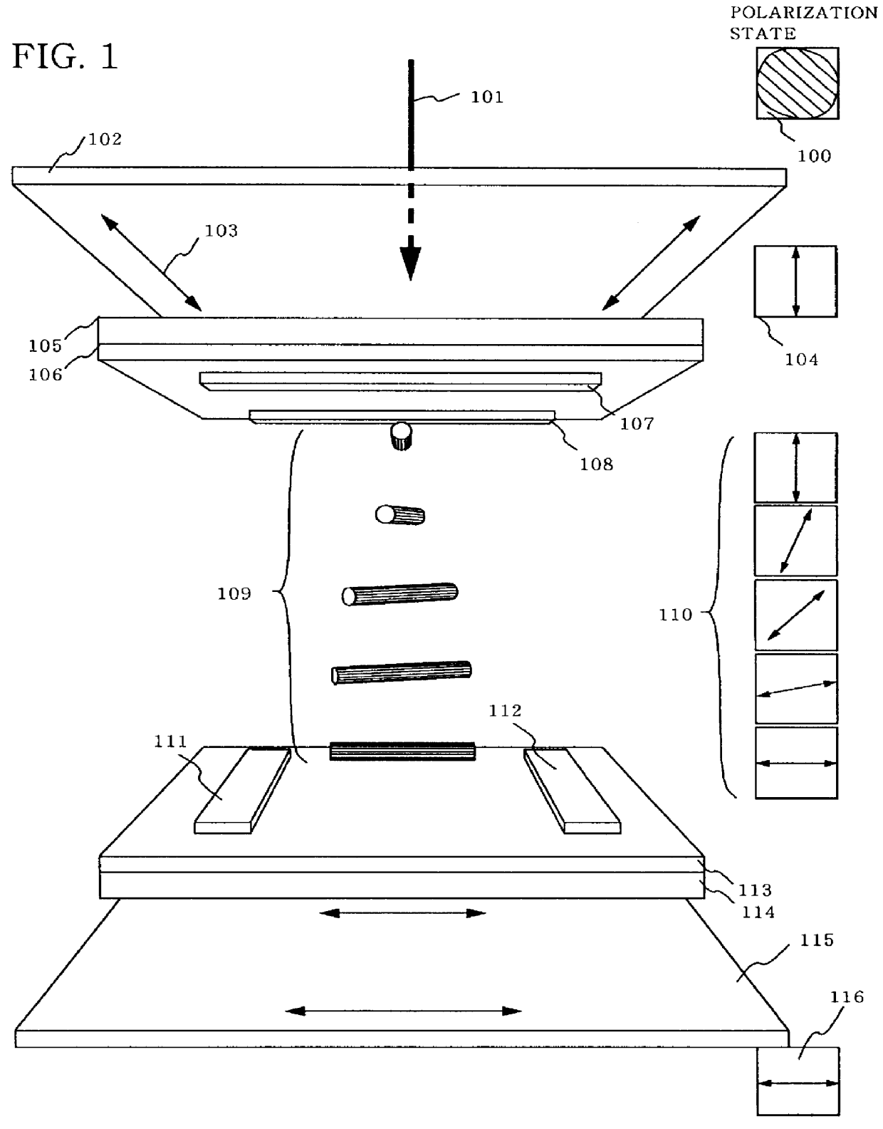
FIG. 1 is a diagrammatic view showing an operation of a liquid crystal panel composed of one pixel constructed by utilizing the invention disclosed in the present specification. This liquid crystal panel may be considered as a liquid crystal shutter for switching whether to transmit or not to transmit incident light. FIG. 1 shows a state in which light enters the liquid crystal panel from the top of the figure. No electric field is applied to a liquid crystal layer 109 in FIG. 1.
At first, a state in which the incident light transmits through the liquid crystal panel will be explained by using FIG. 1. That is, an operation for causing the liquid crystal panel to present a bright state will be explained. It is noted that the present embodiment shows an arrangement of normally white display.
Polarization states of the light seen from the input side (states of the light obtained by seeing the liquid crystal panel from the top of the figure) are shown in boxes on the rig...
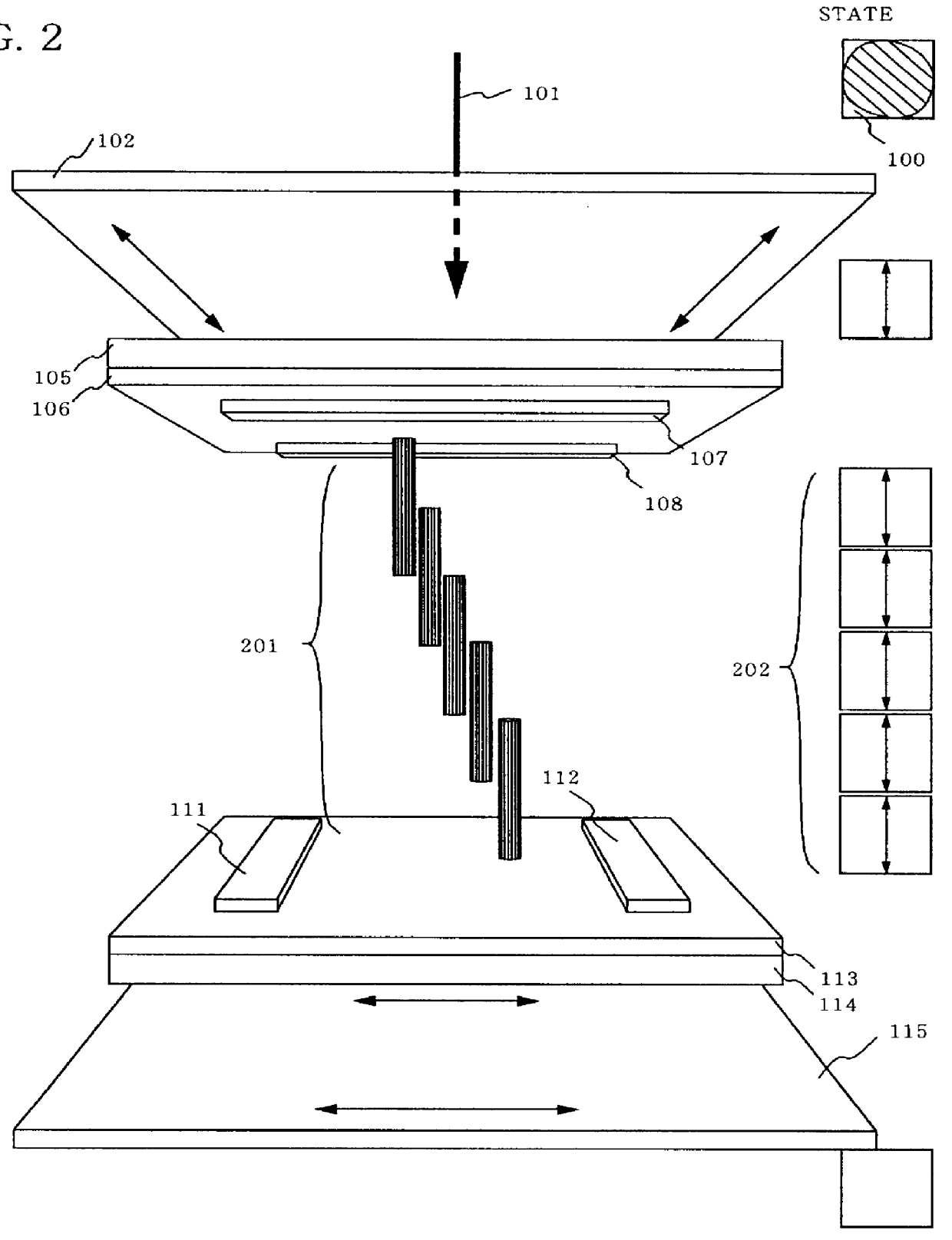
second embodiment
[Second Embodiment]
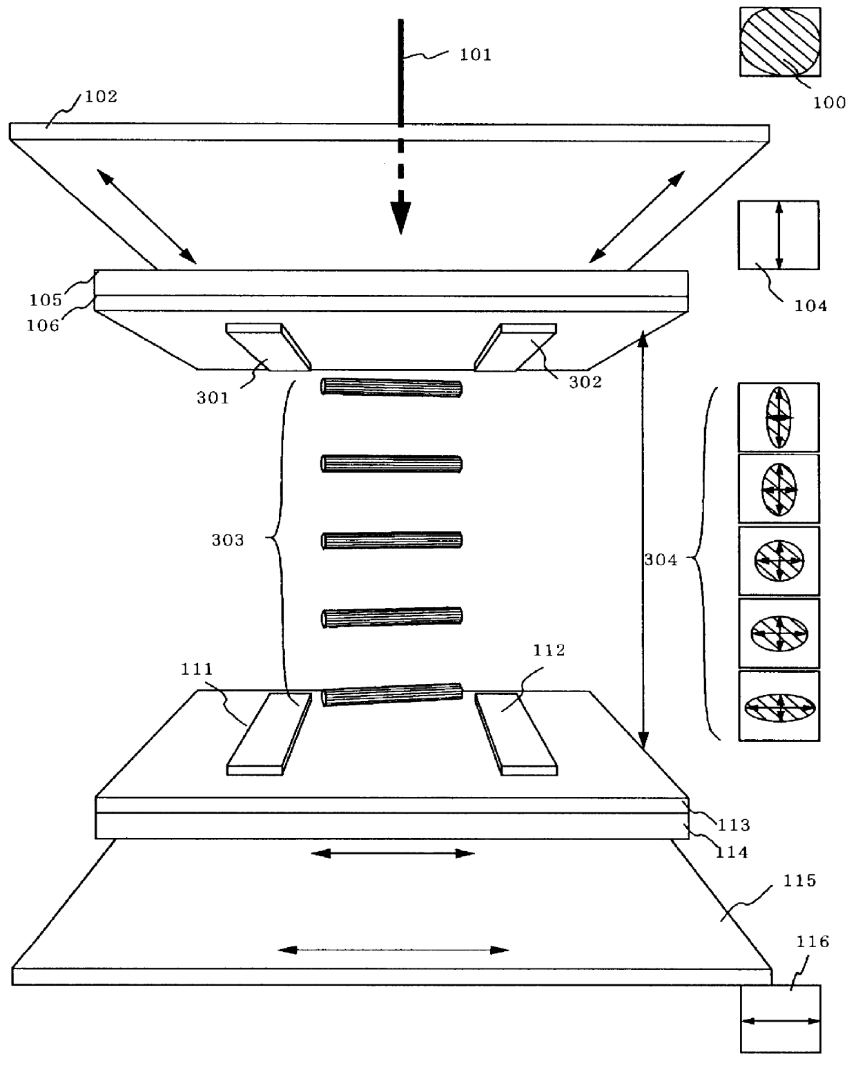
The present embodiment pertains to a display utilizing a double refraction effect. FIG. 3 is a diagrammatic view showing a state in which light transmits through the liquid crystal panel. The state shown in FIG. 3 is the state in which no electric field is applied from the electrodes and the liquid crystal molecules orient in the predetermined direction due to the orientation restricting force. It is noted that the present embodiment presents a case of the liquid crystal panel having the normally white state.
Incident light having a circularly polarized state as shown in the box 100 (state containing all the states is shown as shown in the box 100 for convenience) turns out to be a linearly polarized light as shown in the box 104 as it transmits through the polarizing plate 102.
The incident light having the linearly polarized state as shown in the box 104 enters a liquid crystal layer 303. Here, the liquid crystal layer 303 is set so that an angle made between the ...
third embodiment
[Third Embodiment]
The present embodiment pertains to an arrangement for displaying in normally black in the device which basically performs the TN type operation as shown in the first embodiment.
FIG. 5 is a diagrammatic view of the device in the dark state according to the present embodiment. That is, FIG. 5 shows the state in which the incident light cannot transmit through the liquid crystal panel. The same components of the device with those in FIG. 1 are designated by the same reference numerals.
The arrangement of the present embodiment is different from that shown in FIG. 1 in that the directions of the axes of polarization of the pair of polarizing plates 102 and 501 are the same. It is also different in terms of its operation from the first embodiment shown in FIGS. 1 and 2 in that the bright state and the dark state are reversed.
No electric field is applied from each electrode in the state shown in FIG. 5. In this state, the incident light 101 enters the polarizing plate 102...
PUM
| Property | Measurement | Unit |
|---|---|---|
| electric charge | aaaaa | aaaaa |
| electric field | aaaaa | aaaaa |
| transparent conductive | aaaaa | aaaaa |
Abstract
Description
Claims
Application Information