Substrate cleaning/drying equipment and substrate cleaning/drying method

a technology for cleaning/drying equipment and substrates, which is applied in the direction of cleaning processes and equipment, cleaning using liquids, chemistry apparatus and processes, etc., can solve the problems of difficult control of the etching process and defects in the conduction of the contact portion

Inactive Publication Date: 2000-11-28
KK TOSHIBA
View PDF13 Cites 31 Cited by
  • Summary
  • Abstract
  • Description
  • Claims
  • Application Information

AI Technical Summary

Problems solved by technology

However, if the spin drying is employed after the hydrogen fluoride process, often spot-like foreign matters, each of which is called a water mark, are generated on the surface of the semiconductor substrate.
This water mark acts as a mask in the etching process performed after the water mark has been generated, and thus makes it diffic

Method used


Image

  • Substrate cleaning/drying equipment and substrate cleaning/drying method
  • Substrate cleaning/drying equipment and substrate cleaning/drying method
  • Substrate cleaning/drying equipment and substrate cleaning/drying method

Examples


first embodiment

A first embodiment of the present invention will be explained with reference to FIGS. 4 to 6 hereinbelow. FIG. 4 is a schematic view showing a configuration of a substrate cleaning / drying equipment according to the present invention. The substrate cleaning / drying equipment according to the first embodiment of the present invention executes cleaning and drying of the semiconductor substrate in the same chamber. As shown in FIG. 4, this substrate cleaning / drying equipment comprises a cleaning / drying chamber 27 in which both cleaning and drying of the semiconductor substrate 1 can be carried out. The cleaning / drying chamber 27 has a lid 27a which can be opened and closed arbitrarily on its top portion. This lid 27a is opened when the semiconductor substrate 1 is loaded into the cleaning / drying chamber 27 or the semiconductor substrate 1 is unloaded from the cleaning / drying chamber 27, and is closed to bring the cleaning / drying chamber 27 into sealing condition when the cleaning or dryi...

second embodiment

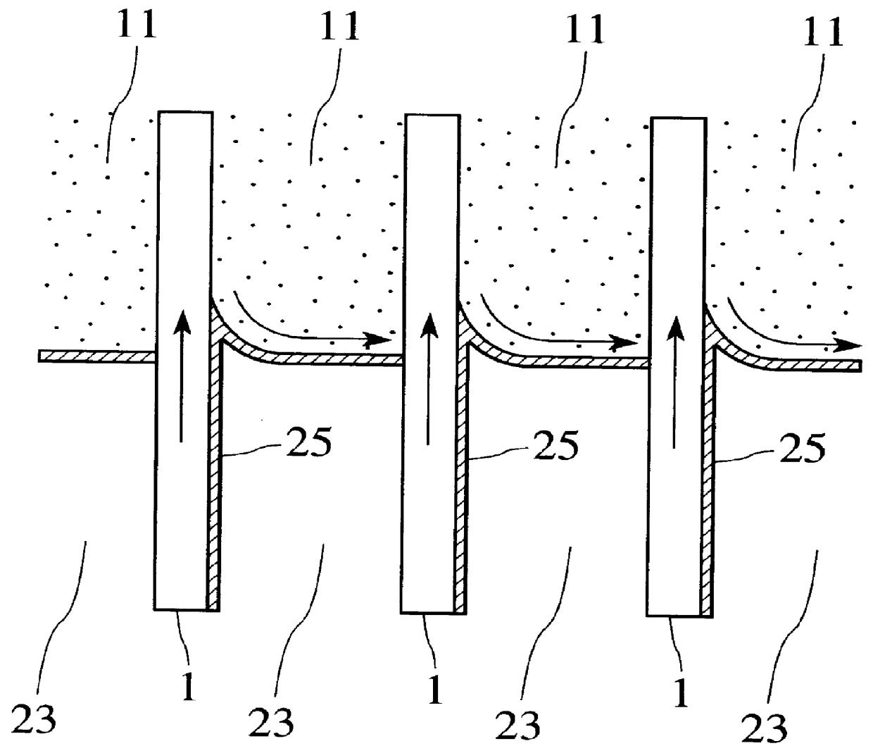
Next, a second embodiment of the present invention will be explained hereinbelow. FIG. 7 is a schematic view showing a configuration of a substrate cleaning / drying equipment according to the second embodiment of the present invention. In the first embodiment shown in FIG. 4, the steam 33 is formed between the ultra pure water 23 in the cleaning tub 17 and the IPA steam 11. In contrast, in this second embodiment of the present invention, when the ultra pure water 23 is discharged via a discharge pipe 35 after the cleaning by using the ultra pure water has been finished, the steam 33 is introduced into the cleaning tub 17 via the steam pipe 29 to mate with a discharge velocity until such steam 33 is filled in the cleaning tub 17. That is, the semiconductor substrates 1 can be passed through the steam 33 having a sufficient width. Unless the width of the steam 33 between the ultra pure water 23 and the IPA steam 11 is sufficient, there is a possibility that movement of the silica group...

third embodiment

Next, a third embodiment of the present invention will be explained hereinbelow. FIG. 8 is a schematic view showing a configuration of a substrate cleaning / drying equipment according to the third embodiment of the present invention. The third embodiment of the present invention comprises a steam nozzle 37 for injecting the steam onto the semiconductor substrate 1, and an IPA steam nozzle 39 for injecting the IPA steam onto the semiconductor substrate 1. The steam nozzle 37 and the IPA steam nozzle 39 are connected to a steam supply source and an IPA steam supply source respectively via valves, regulators, etc. As shown in FIG. 8, in the third embodiment, when the semiconductor substrates 1 are pulled up from the ultra pure water 23, the steam 33 being injected from the steam nozzle 37 is placed over the ultra pure water 23 and also the IPA steam 11 being injected from the IPA steam nozzle 39 is placed over the steam being injected from the steam nozzle 37. Therefore, like the first ...


PUM


Abstract

There is provided a substrate cleaning/drying equipment for removing residual moisture from a substrate by exposing the substrate to an IPA steam after the substrate has been cleaned by a ultra pure water. The substrate cleaning/drying equipment comprises a cleaning/drying chamber for cleaning/drying the substrate, a cleaning tub which is provided below the cleaning/drying chamber and to which at least a ultra pure water is supplied, an IPA steam supplying pipe for supplying the IPA steam to an upper area of the cleaning/drying chamber such that the upper area of the cleaning/drying chamber is filled with the IPA steam, a steam supplying pipe for supplying a steam between the ultra pure water in the cleaning tub and the IPA steam, and a carrying unit for carrying the substrate, which has been cleaned by the ultra pure water, from the ultra pure water into the IPA steam via the steam. The ultra pure water, the steam, the IPA steam may be supplied onto the substrate by using injection nozzles respectively in order of the ultra pure water, the steam, the IPA steam.

Description

1. Field of the InventionThe present invention relates to an equipment and a method for cleaning and drying a substrate. More particularly, the present invention relates to an equipment and a method for cleaning and drying various substrates such as a semiconductor substrate in semiconductor device manufacturing steps, a reticle (photomask) in a lithography step as one of the semiconductor device manufacturing steps, a flat panel in liquid crystal display manufacturing steps, etc.2. Description of the Related ArtIn order to clean the surface of the semiconductor substrate on which semiconductor devices are formed, etc., the cleaning step of the semiconductor substrate and the drying step following to the cleaning step are frequently repeated in the semiconductor device manufacturing steps. Especially, in order to form a silicon oxide film of high quality, it is essential to implement a ultra clean surface on the surface of the semiconductor substrate. Therefore, an oxide film on the...

Claims


Application Information

Patent Timeline
IPC IPC(8): H01L21/00H01L21/304
CPCH01L21/67028Y10S134/902
Inventor TAKASE, KAZUHIKOFUKAZAWA, YUJI
Owner KK TOSHIBA
Why Eureka
Try Eureka