

Video signal processing circuit inhibiting display of distorted images
a video signal processing and image technology, applied in the field of video signal processing circuits, can solve the problems of affecting the current display image, affecting the presently displayed image, and changing the reduction ratio with time distortion between the write side and the read sid
- Summary
- Abstract
- Description
- Claims
- Application Information
AI Technical Summary
Problems solved by technology
Method used
Image

Examples
first embodiment
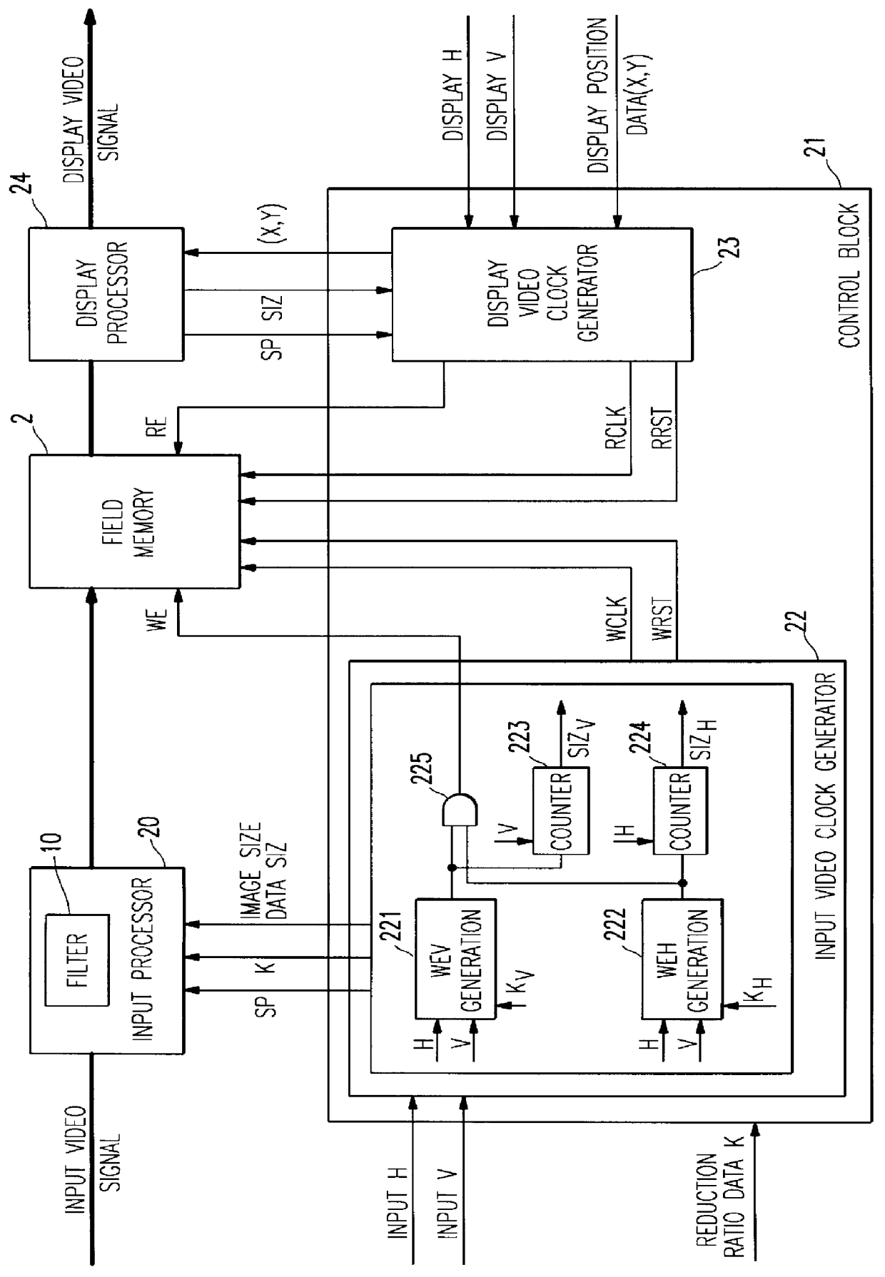
FIG. 1 is a block diagram showing the invention;
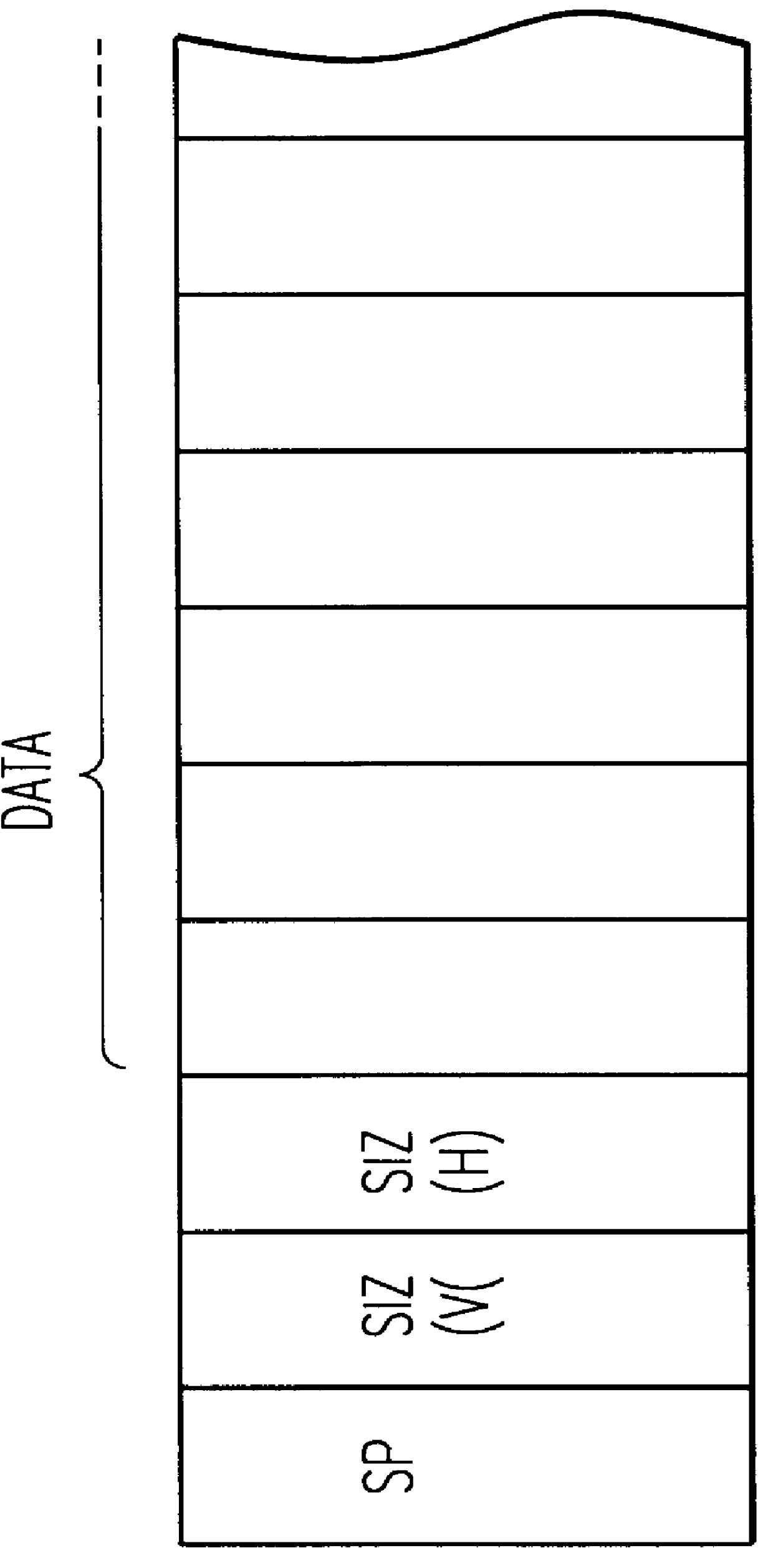
FIG. 2 is an explanatory diagram showing a data format to be written in a field memory;
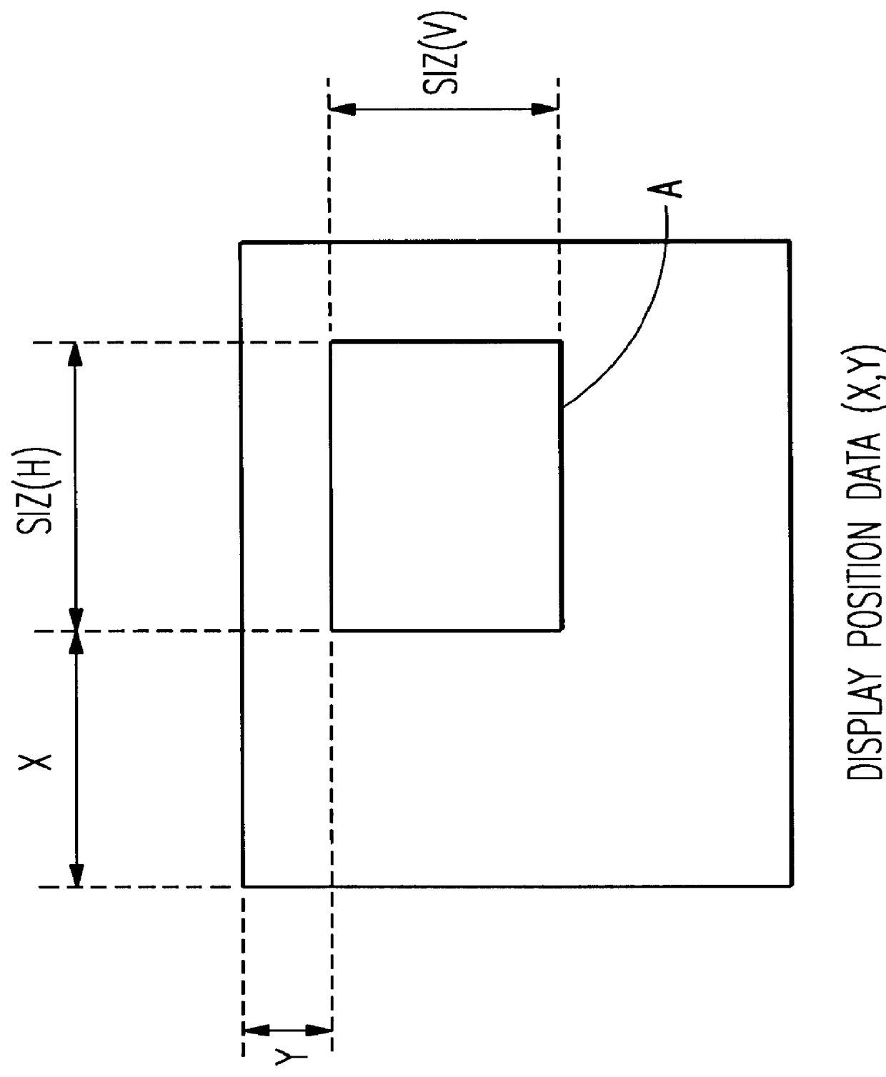
FIG. 3 is a diagram showing an example of a window display;
FIG. 4 is a timing chart for illustrating operation of the first embodiment;
FIG. 5 is a timing chart for illustrating actions of the case in which an address pass occurs in the embodiment of FIG. 1;
FIG. 6 is a block diagram showing a second embodiment of the invention;
FIG. 7 is a timing chart for illustrating operation of the second embodiment;
FIG. 8 is a timing chart for illustrating the actions of the case in which an address pass occurs in the second embodiment;
FIG. 9 is a block diagram showing a conventional reduced video signal processing circuit;
FIG. 10 is a timing chart for illustrating operation of the reduced video signal processing circuit;
FIG. 11 is a diagram showing an example of a conventional window display; and
FIG. 12 is a timing chart for explaining other actions of the reduce...
second embodiment
the present invention which utilizes a shorter muting period is shown in FIG. 6. In this second embodiment, an input video clock generator 25 is constructed to output a write inhibiting signal WESP, as shown at (b) in FIG. 7, only for the one-field period just after the change in the reduction ratio data K. There is further provided an AND gate 26 which receives the inverted output of the write inhibiting signal WESP and the enable signal WE and outputs the enable signal WE1 in response. Consequently, as shown in a timing chart of FIG. 7, the enable signal WE1, as shown at (d) in FIG. 7, is not outputted and the header and the video signals are not written in the field memory for the one-field period just after NP2, as shown at (a) in FIG. 7, of the change in the reduction ratio. As a result, for the one-field period preceding DP2, as shown at (e) in FIG. 7, there are read out the header and the video signal which are written for the one-field period just before NP2. Since the heade...
PUM
 Abstract
Description
Claims
Application Information