Power supply insensitive substrate bias voltage detector circuit

a technology of bias voltage and detector circuit, which is applied in the direction of electric variable regulation, process and machine control, instruments, etc., can solve the problems of affecting the operation of the device, affecting the accuracy of the signal, and consuming more static power

Inactive Publication Date: 2001-01-09
PROMOS TECH INC
View PDF6 Cites 12 Cited by
  • Summary
  • Abstract
  • Description
  • Claims
  • Application Information

AI Technical Summary

Problems solved by technology

The increased junction leakage adversely impacts the operation of the device.
For example, in a DRAM the increased junction leakage can cause loss of information stored in the memory cells; and more generally, the high leakage current results in higher static power consumption, e.g., high stand-by current (I.sub.SB).
The undesirable effects of the large leakage currents, such as high I.sub.SB and data loss in DRAM cells, are magnified as technology moves to smaller geometries and memory devices move to higher densities.
Another drawback of circuit 17 (FIG. 1) is that it does not prevent V.sub.BB from becoming positive.
This can lead to latch-up which may destroy the device.
Thus, some V.sub.BB generators include a circuit that allows V.sub.BB to get arbitrarily close to 0 volts but does not allow V.sub.BB to become positive.

Method used


Image

  • Power supply insensitive substrate bias voltage detector circuit
  • Power supply insensitive substrate bias voltage detector circuit
  • Power supply insensitive substrate bias voltage detector circuit

Examples


Embodiment Construction

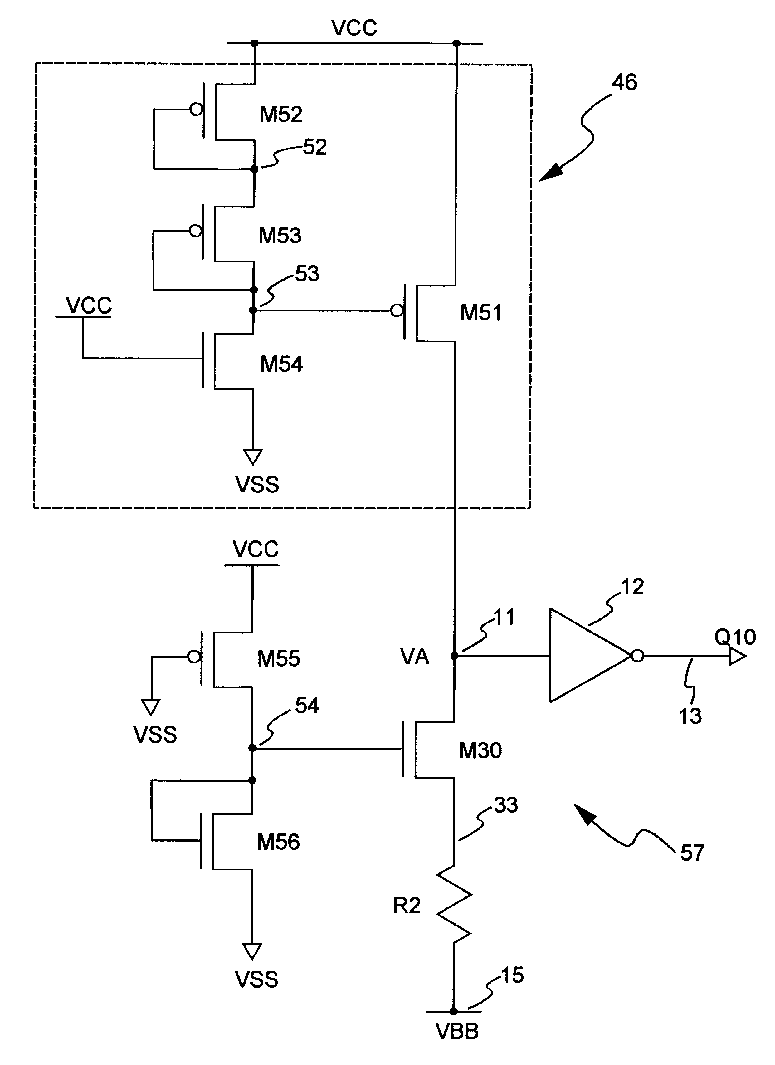
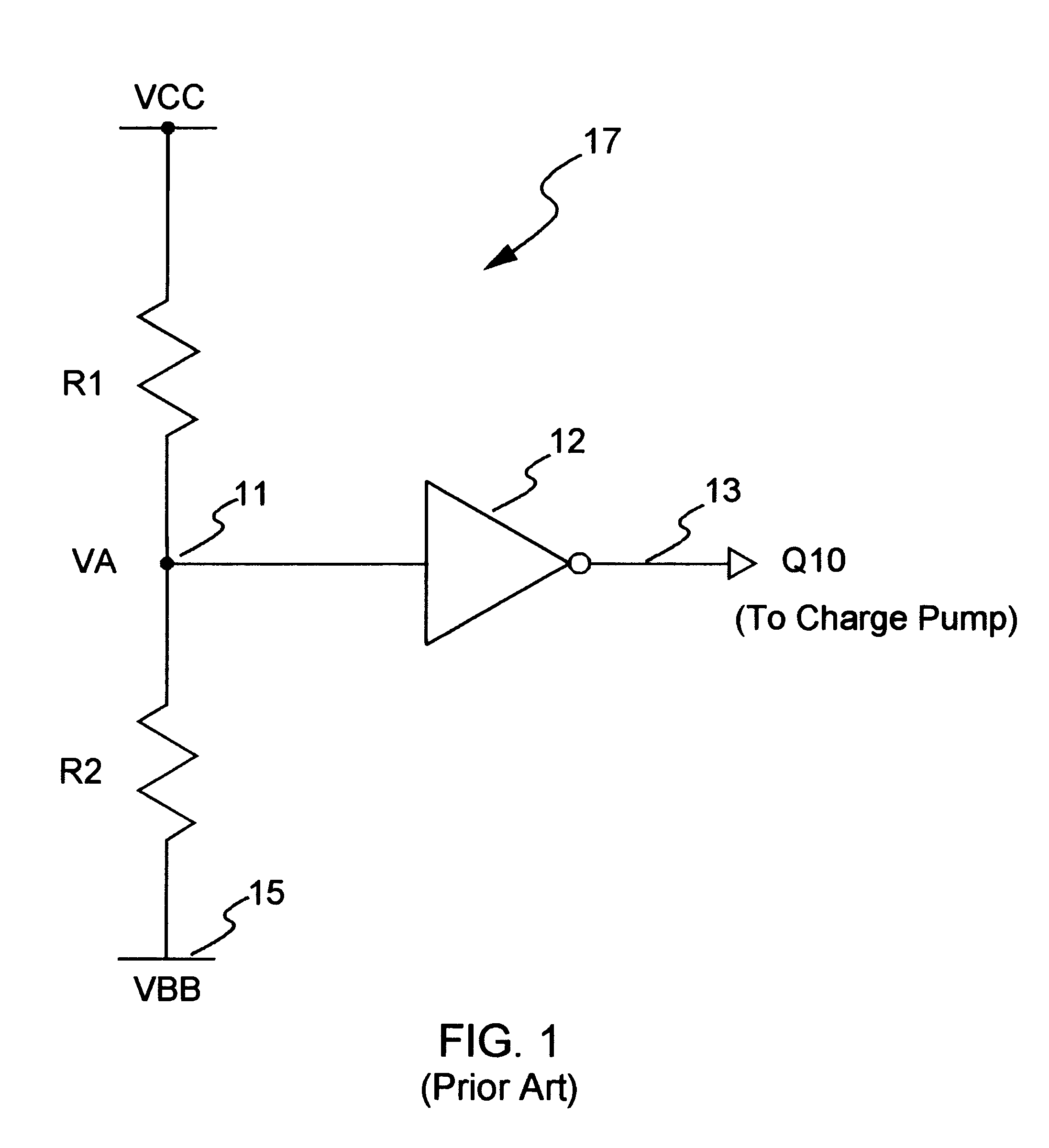
FIG. 4A shows a voltage detector circuit 47 in accordance with the present invention. The resistor R1 of FIG. 1 is replaced with a power-supply-voltage-insensitive current source 46. The current source 46 is connected between Vcc and node 11. Resistor R2 is connected between node 11 and V.sub.BB terminal 15 (note that R2 may be implemented using a MOS transistor, or a strip of polysilicon, or a strip of diffusion). Inverter 12 has its input terminal connected to node 11, and its output terminal represents the output terminal Q10 of the detector circuit 47. The output terminal Q10 is connected to an input terminal 13 of a charge pump 48. The charge pump 48 provides the voltage V.sub.BB on terminal 15.

The operation of circuit 47 is similar to that of circuit 17 in FIG. 1. However, by replacing R1 (FIG. 1) with the current source 46, the operation of the detector circuit 47 is made insensitive to Vcc variations. This is because the current source 46 provides a constant current despite ...


PUM


Abstract

In accordance with the present invention, a circuit provides a bias voltage V1 which is substantially insensitive to variations of a power supply voltage powering the circuit. The circuit includes a detector circuit for generating a signal from the power supply voltage and the bias voltage V1, wherein the signal is substantially insensitive to variations in the power supply voltage while being responsive to the bias voltage V1. The circuit further includes a voltage generator circuit for generating the bias voltage V1 wherein the voltage generator is responsive to the signal such that the detector circuit and the voltage generator maintain the bias voltage V1 at a substantially constant value over power supply voltage variations. The detector circuit also includes a circuit for allowing bias voltage V1 to get arbitrarily close to the ground voltage but not allowing the bias voltage V1 to become positive.

Description

1. Field of the InventionThe present invention relates to providing voltages.2. Description of Related ArtVoltage generating circuits are widely used in electrical and electronic devices. For instance, substrate bias generator circuits, also referred to as back-bias generators, are used in semiconductor devices which require the substrate region to be biased to a predetermined voltage. For example, in dynamic random access memories (DRAM) the substrate region is negatively biased to prevent the DRAM cells from losing the stored information. The back-bias generator includes a voltage multiplier circuit, commonly referred to as charge pump, for providing the negative Back-Bias Voltage (V.sub.BB). The charge pump is usually accompanied by a V.sub.BB detector circuit. The detector circuit regulates the charge pump such that V.sub.BB is maintained as close to a target V.sub.BB value as possible.The detector circuit constantly senses the V.sub.BB voltage level, and if V.sub.BB becomes mor...

Claims


Application Information

Patent Timeline
Patent Type & Authority Patents(United States)
IPC IPC(8): G05F3/08G05F3/20
CPCG05F3/205
Inventor YOUNG, POCHUNGLI, LI-CHUN
Owner PROMOS TECH INC
Why Eureka
Try Eureka