Semiconductor memory device with internal voltage generators for testing a memory array and peripheral circuits

a memory array and peripheral circuit technology, applied in the field of semiconductor integrated circuit devices, can solve the problems of not being able to detect defects in devices produced, reducing the probability of stored data changing during read operations, and manufacturing defects in such memory cells. the effect of improving the burn-in test

Inactive Publication Date: 2005-10-25
SAMSUNG ELECTRONICS CO LTD
View PDF6 Cites 90 Cited by
  • Summary
  • Abstract
  • Description
  • Claims
  • Application Information

AI Technical Summary

Benefits of technology

[0008]In an exemplary embodiment, the present invention provide a se

Problems solved by technology

However, the cross-coupled nature of SRAM cells may result in manufacturing defects in such memory cells.
Such defects may not be detectable when a device is produced, but may manifest themselves after time.
In other words, the lar

Method used


Image

  • Semiconductor memory device with internal voltage generators for testing a memory array and peripheral circuits
  • Semiconductor memory device with internal voltage generators for testing a memory array and peripheral circuits
  • Semiconductor memory device with internal voltage generators for testing a memory array and peripheral circuits

Examples


Embodiment Construction

[0025]Exemplary embodiments of the present invention will be more fully described with reference to the attached drawings.

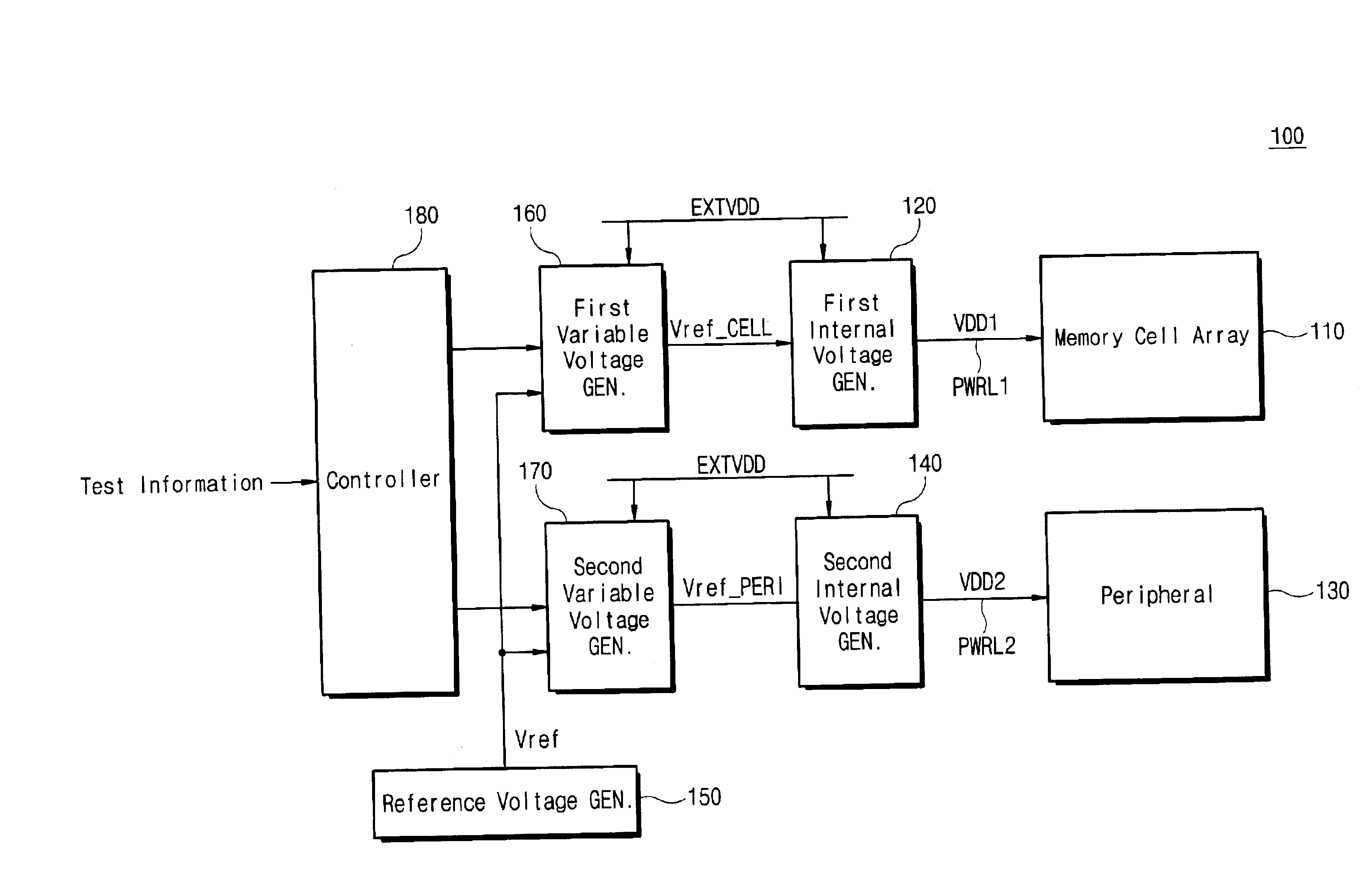
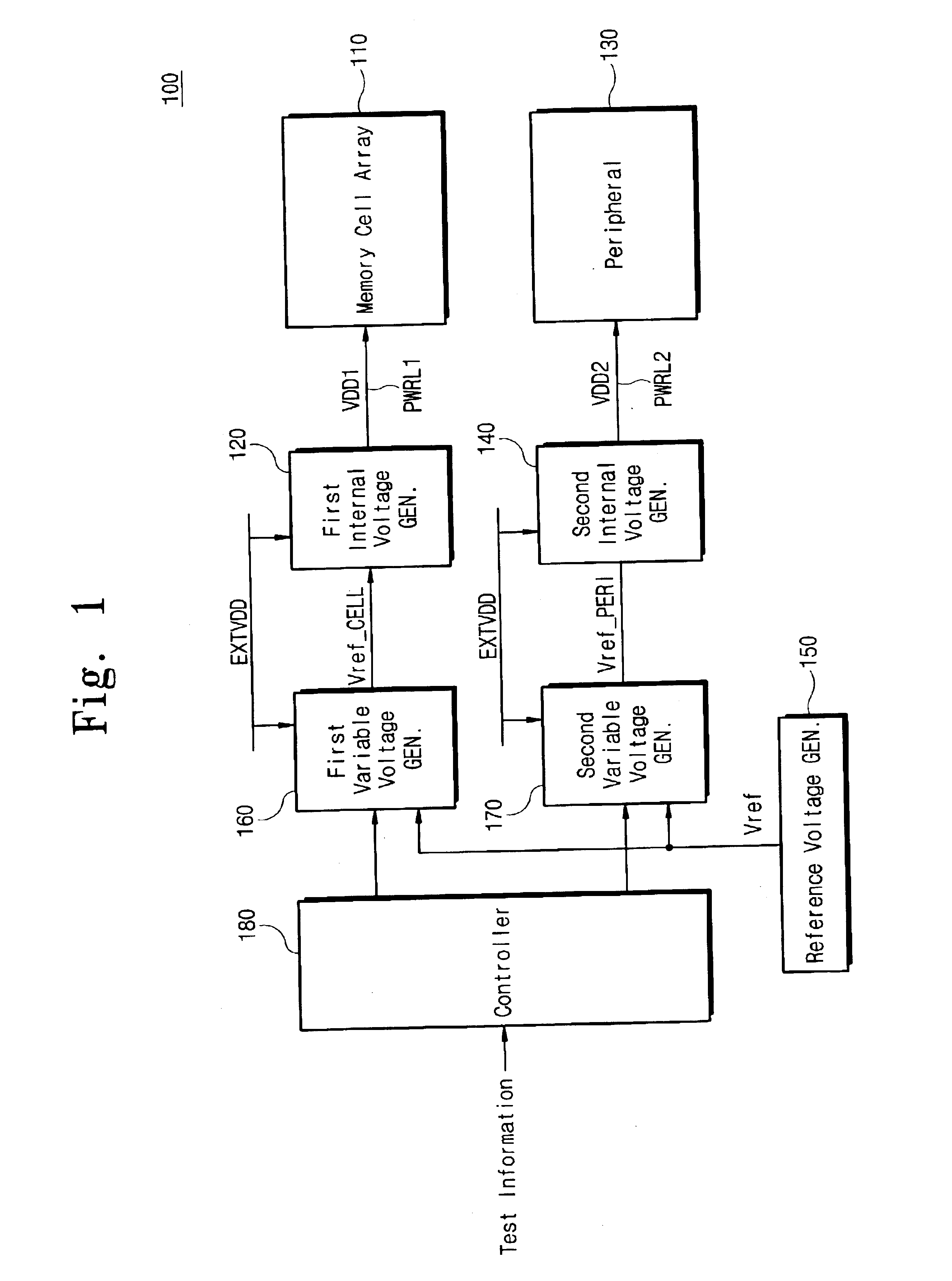
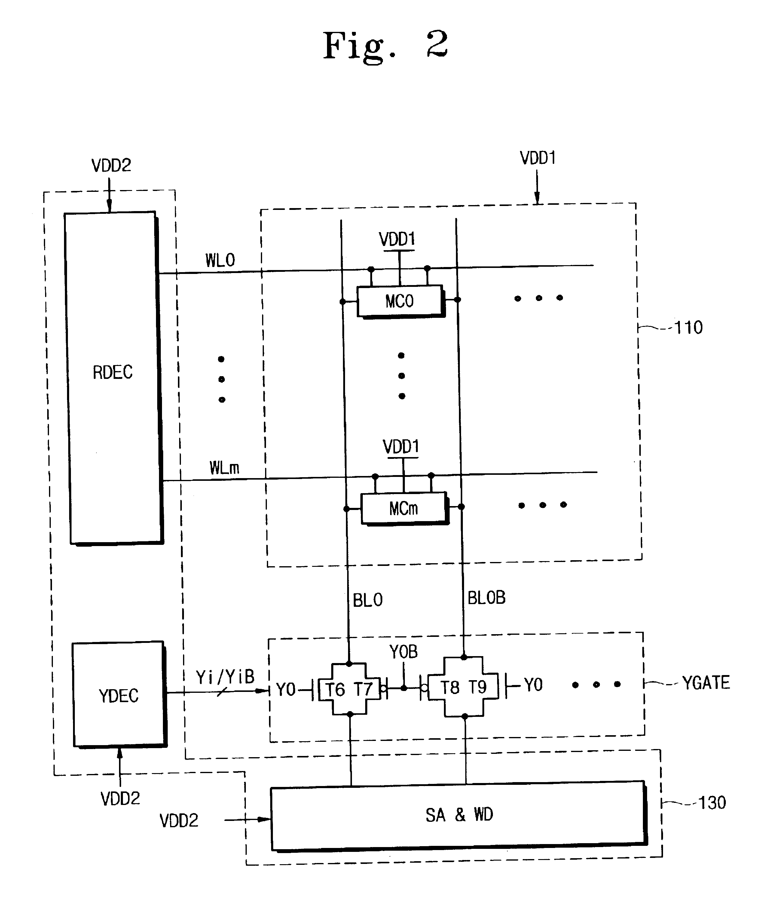
[0026]FIG. 1 illustrates a semiconductor memory device according to an exemplary embodiment of the present invention. Referring to FIG. 1, a semiconductor memory device 100 according to an exemplary embodiment of the present invention is an SRAM device, but it is obvious that the spirit of the invention can be applied to other types of memory devices, for example, DRAM, FRAM, EEPROM, etc. The semiconductor memory device 100 includes a memory cell array 110 for storing data information, and is supplied with a first internal power supply voltage VDD1 from a first internal voltage generator circuit 120 via a power supply line PWRL1. A peripheral circuit 130 is supplied with a second internal power supply voltage VDD2 from a second internal voltage generator circuit 140 via a power supply line PWRL2. The peripheral circuit 130 controls read and write operations of th...


PUM


Abstract

A semiconductor memory device which includes an internal voltage generator circuit for adjusting an external power supply voltage and generating first and second internal power supply voltages. The first internal power supply voltage is supplied to a memory cell array via a first power supply line, and the second internal power supply voltage is supplied to a peripheral circuit via a second power supply line. A control circuit controls the internal voltage generator circuit so that the levels of the first and second internal power supply voltages vary depending on a mode of operation.

Description

[0001]This U.S. nonprovisional patent application claims priority under 35 U.S.C. §119 upon Korean Patent Application No. 2002-44983, filed on Jul. 30, 2002, the contents of which are herein incorporated by reference in their entirety.FIELD OF THE INVENTION[0002]The present invention is related to a semiconductor integrated circuit device, and in particular, to a semiconductor memory device which is capable of testing the reliability of memory cells.BACKGROUND OF THE INVENTION[0003]A static random access memory (SRAM) device includes more metal oxide semiconductor field effect transistors than a conventional dynamic random access memory (DRAM) device, and can store data without refreshing. However, the cross-coupled nature of SRAM cells may result in manufacturing defects in such memory cells. Such defects may not be detectable when a device is produced, but may manifest themselves after time. Such memory cells are referred to as memory cells having a potential defect property.[0004...

Claims


Application Information

Patent Timeline
IPC IPC(8): G11C5/14G11C29/12G11C29/04G11C29/50
CPCG11C5/147G11C29/12G11C29/12005G11C29/50G11C11/41G11C2207/2254G11C5/14
Inventor PARK, CHUL-SUNGYANG, HYANG-JALEE, SEUNG-MINNOH, YONG-HWAN
Owner SAMSUNG ELECTRONICS CO LTD
Why Eureka
Try Eureka