

Multi-layer circuit board
a multi-layer circuit board and circuit board technology, applied in the direction of printed circuit aspects, basic electric elements, solid-state devices, etc., can solve the problems of increasing technical difficulty, serious problems in the yield of products, reliability and production cost, and no longer being able to take out the wiring from every land on the surfa
Inactive Publication Date: 2001-02-27
SHINKO ELECTRIC IND CO LTD
View PDF8 Cites 49 Cited by
- Summary
- Abstract
- Description
- Claims
- Application Information
AI Technical Summary
Problems solved by technology
When the electrodes are arranged in many sequences on the electrode-forming surface, however, it becomes no longer possible to take out the wiring from every land on the surface though it may vary depending upon the distance between the lands and the number of the lands.
When the circuit boards on which the circuit patterns are very densely formed are to be laminated in many layers, there will be employed a high-density wiring method such as build-up method accompanied, however, by serious problems in regard to yield of the products, reliability
Method used
View moreImage
Smart ImageViewing Examples

Examples
 PUM
 Abstract
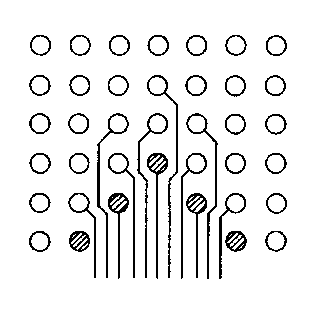
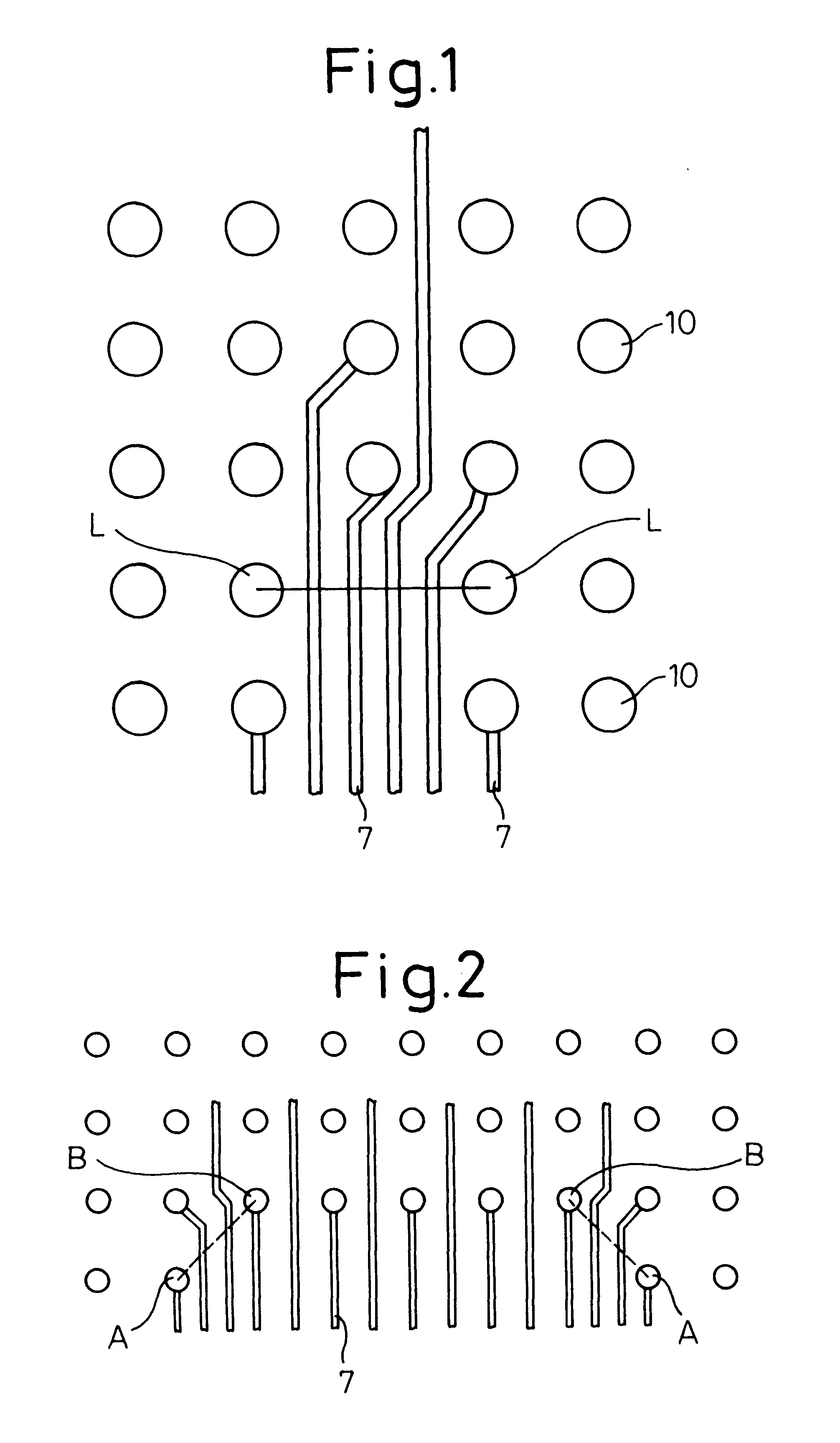
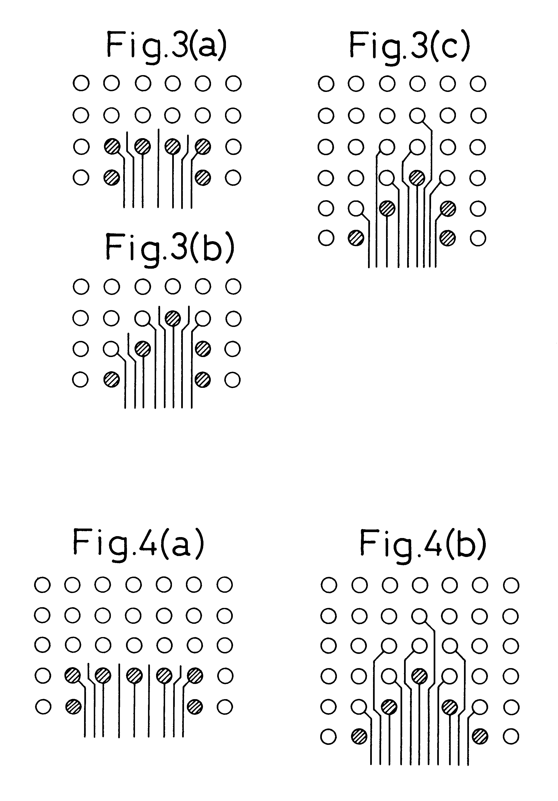
A multi-layer circuit board formed by laminating a plurality of circuit boards each having lands arranged in many number in the form of a lattice or in a staggering manner on the side of the mounting surface and having circuit patterns with the ends on one side thereof being connected to said lands and with the ends on the other side thereof being drawn toward the outside from a region where said lands are arranged; wherein the lands for drawing the circuit patterns in a number not less than a+1 are arranged on the oblique lines of an isosceles triangle having a base formed by consecutive lands of a number of n and having oblique lines in the diagonal directions, the value n satisfying m>=k+1 of the two values of:wherein "a" is the number of the circuit patterns that can be arranged between the neighboring lands on the circuit board, and "n" is a parameter.
Description
1. Field of the InventionThe present invention relates to a multi-layer circuit board for mounting an electronic element such as a semiconductor chip having connection electrodes arranged in the form of a lattice or a semiconductor device having external connection terminals arranged in an area array form.2. Description of the Related ArtIn modern semiconductor devices, the logic devices are becoming highly functional and highly integrated, feature more inputs and outputs, and are being mounted ever more densely. Therefore, products have been produced, to compensate for a lack of space for forming electrodes, by arranging electrodes like a lattice on the electrode-forming surface of a semiconductor chip.FIG. 26 illustrates an example in which a semiconductor chip 4 is mounted on a circuit board 5 relying on an ordinary flip chip connection. The semiconductor chip 4 has electrodes 6 arranged on the peripheral edges thereof. Circuit patterns 7 are connected to every electrode 6 on a s...
Claims
Login to View More Application Information
Patent Timeline
 IPC IPC(8): H01L23/498H01L23/48H05K1/11H05K1/00H01L23/12H01L21/60H05K3/46
CPCH01L23/49822H01L23/49838H05K1/112H01L2224/16H01L2924/15174H01L2924/15311H01L2224/16235H05K2201/09227H05K2201/10734H01L2924/01019H05K1/0298H01L23/538
InventorHORIUCHI, MICHIOTAKEUCHI, YUKIHARUYODA, EIJI
OwnerSHINKO ELECTRIC IND CO LTD