Package having very thin semiconductor chip, multichip module assembled by the package, and method for manufacturing the same

a very thin, semiconductor chip technology, applied in semiconductor devices, semiconductor/solid-state device details, electrical apparatus, etc., can solve the problems of reducing thickness, cracking of mcm, and weak mechanical strength of the package itsel

Inactive Publication Date: 2001-05-29
KK TOSHIBA
View PDF15 Cites 261 Cited by
  • Summary
  • Abstract
  • Description
  • Claims
  • Application Information

AI Technical Summary

Problems solved by technology

However, because the height of the package from its mounting face of the MCM substrate is quite high, the MCM shown in FIG. 1 is not capable of satisfying the recent demands such as the reduction in thickness.
However, although the entire thickness of the package was able to reduced towards less than 200 .mu.m by using the structure of the semiconductor package shown in FIG. 2, the mech

Method used


Image

  • Package having very thin semiconductor chip, multichip module assembled by the package, and method for manufacturing the same
  • Package having very thin semiconductor chip, multichip module assembled by the package, and method for manufacturing the same
  • Package having very thin semiconductor chip, multichip module assembled by the package, and method for manufacturing the same

Examples


Embodiment Construction

Various modifications will become possible for those skilled in the art after receiving the teachings of the present disclosure without departing from the scope thereof.

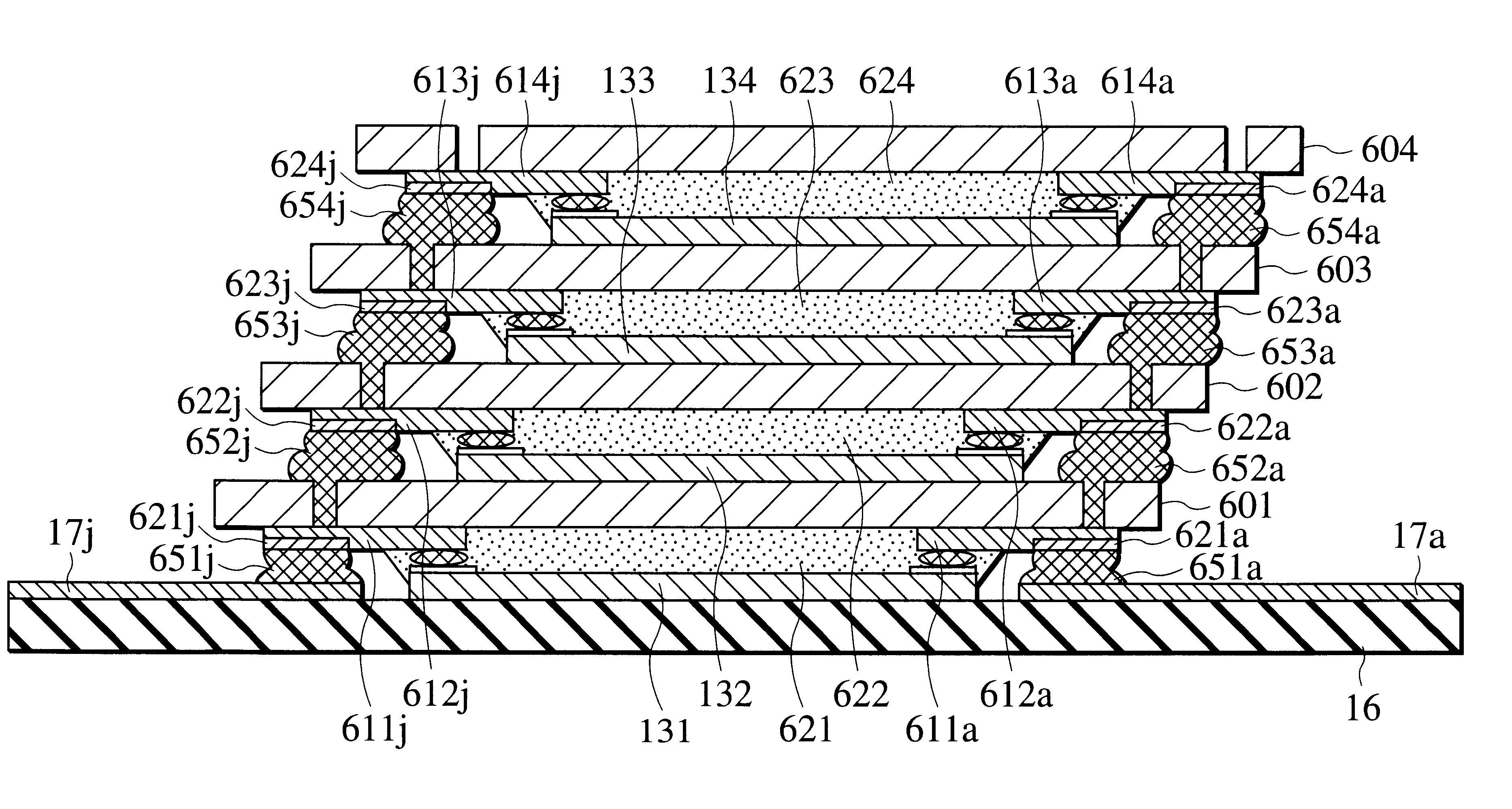
It is permissible to laminate the semiconductor packages, each of which is shown in FIG. 8A, having a structure of the second embodiment, in the stacked configuration of the first embodiment, namely, such that the top and bottom surfaces of the thin semiconductor packages are inverted and predetermined electrodes are electrically connected.

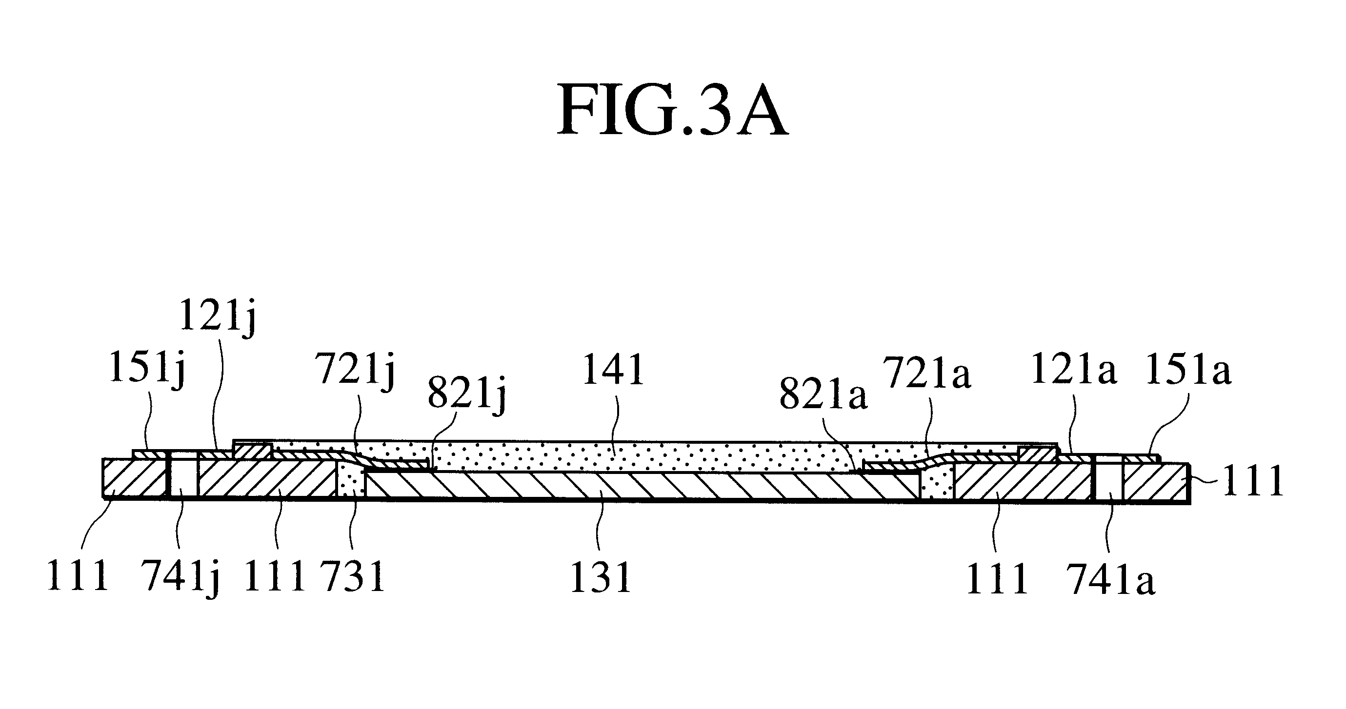
On the contrary, it is also permissible to laminate the semiconductor packages as shown in FIG. 3A, having a structure according to the first embodiment, in the stacked configuration of the second embodiment, namely, such that they are shifted in the direction of the plane and predetermined electrodes are electrically connected to each other. In this case, it is preferable to prepare the flat oval-shaped connection lands 851j, 851k, 851l, 851m, . . . , each having major axis along ...


PUM


Abstract

A semiconductor package of this invention has an insulating substrates, wiring layers disposed on the surface of the insulating substrate, a semiconductor chip disposed in a device hole provided in the insulating substrate, inner-joint-conductors for connecting at least part of the bonding pads on the surface of the semiconductor chip to the corresponding inner-joint-conductors and connection lands connected to the wiring layers. The device hole is provided so that it goes through the center of the insulating substrate. The semiconductor chip is thinner than the insulating substrate. Then, this semiconductor chip is disposed in the device hole such that a bottom thereof is flush with a bottom plane of the insulating substrate. Further, this invention provides a MCM in which plural pieces of the thin semiconductor packages are laminated. In the MCM, the semiconductor packages are laminated such that top and bottom faces of the thin silicon chip are inverted. Predetermined connection lands are electrically connected to each other through a connecting conductor. This MCM has a high mechanical strength in its stacked structure and there is a low possibility that crack may occur in the package due to stress in the bending direction.

Description

1. Field of the InventionThe present invention relates to a very thin semiconductor package mounting a very thin semiconductor chip, multichip module (MCM) in which plural pieces of the very thin semiconductor packages are laminated, and manufacturing method for the same very thin semiconductor package and MCM.2.Description of the Related ArtFIG. 1 is a cross sectional view of a conventional MCM in which the semiconductor packages are laminated. This MCM has a structure in which two semiconductor packages are laminated by tape carrier package (TCP) architecture in a space having a restricted height. In the lower TCP, Cu wiring layers 104a, 104j are disposed on a polyimide film 101, which is an insulating substrate. End portions of the Cu wiring layers 104a, 104j are connected to inner leads 203a, 203j. The inner leads 203a, 203j are connected to bonding pads of a silicon chip 94. Further, the silicon chip 104 is bonded to the insulating substrate 101 with insulating adhesive (not sh...

Claims


Application Information

Patent Timeline
IPC IPC(8): H01L23/28H01L21/56H01L21/67H01L23/31H01L21/02H01L21/68H01L25/10H01L25/18H01L23/12H01L25/11
CPCH01L21/563H01L23/3107H01L25/105H01L24/29H01L21/6836H01L2225/1058H01L2221/68327H01L2223/54473H01L2224/16225H01L2224/73203H01L2224/73204H01L2224/83192H01L2924/01004H01L2924/01005H01L2924/01015H01L2924/01029H01L2924/01032H01L2924/01047H01L2924/01049H01L2924/01079H01L2924/01082H01L2924/10329H01L2924/14H01L2924/01006H01L2924/01019H01L2924/01023H01L2924/01033H01L2924/01087H01L2924/0132H01L2225/1035H01L2924/07802H01L2224/32225H01L2224/45147H01L2924/00014H01L2924/10253H01L2225/1023H01L2924/01022H01L2924/01028H01L2924/3512H01L2924/00H01L2224/48H01L2224/05568H01L2224/05573H01L2924/00011H01L2224/05599H01L23/12
Inventor ASADA, JUNICHI
Owner KK TOSHIBA
Why Eureka
Try Eureka