Integrated circuit output buffers having feedback switches therein for reducing simultaneous switching noise and improving impedance matching characteristics

a technology of input buffers and feedback switches, which is applied in logic circuits, pulse techniques, and reliability increasing modifications, etc., can solve problems such as increasing buffer cell area and power consumption

Inactive Publication Date: 2001-06-05
INTEGRATED DEVICE TECH INC
View PDF65 Cites 26 Cited by
  • Summary
  • Abstract
  • Description
  • Claims
  • Application Information

AI Technical Summary

Problems solved by technology

There is a tradeoff, however, since the introduction of the additional PMOS transistor and inverter INV15 will increase buffer cell area and power consumption.

Method used


Image

  • Integrated circuit output buffers having feedback switches therein for reducing simultaneous switching noise and improving impedance matching characteristics
  • Integrated circuit output buffers having feedback switches therein for reducing simultaneous switching noise and improving impedance matching characteristics
  • Integrated circuit output buffers having feedback switches therein for reducing simultaneous switching noise and improving impedance matching characteristics

Examples


first embodiment

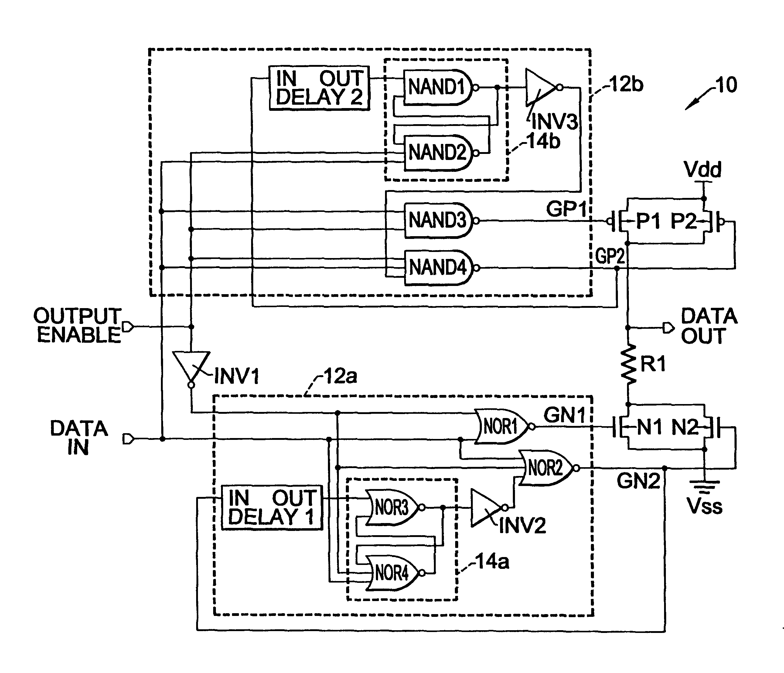
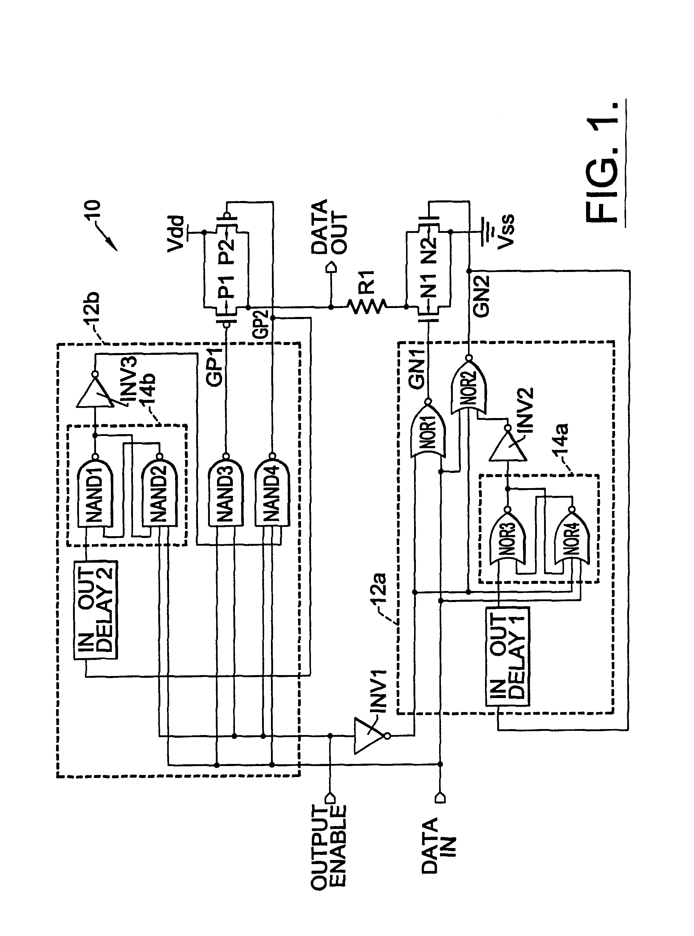
Referring now to FIGS. 1-2, an integrated circuit output buffer 10 according to the present invention passes an input signal (DATA IN) as an output signal (DATA OUT) with low propagation delay when the buffer 10 is enabled (i.e., OUTPUT ENABLE=1) and generates a high impedance output state when the buffer is disabled (OUTPUT ENABLE=0). The preferred buffer 10 includes first and second pull-down switches that are electrically connected in parallel. As illustrated, the first and second pull-down switches may comprise NMOS pull-down transistors N1 and N2. These pull-down transistors each have first terminals (drain electrodes) that are electrically connected to an output signal line (DATA OUT) by a resistor R1. This resistor R1 provides electrostatic discharge (ESD) protection and may have a value of about 10.OMEGA., for example. The second terminals (i.e., source electrodes) of the pull-down transistors N1 and N2 are also electrically connected to a first reference signal line (e.g., ...

second embodiment

Referring now to FIGS. 3-4, an integrated circuit output buffer according to the present invention includes a pull-down circuit 20a and a pull-up circuit 20b. As illustrated, the pull-down circuit 20a includes first and second pull-down switches that are electrically connected in parallel. These first and second pull-down switches may be provided by NMOS pull-down transistors N3 and N4 that are electrically connected to an output signal line (DATA OUT) by a resistor R3. This resistor R3 provides electrostatic discharge (ESD) protection and may have a value of about 10.OMEGA., for example. A pull-down control circuit 22a is also provided to control the turn-on and turn-off of the pull-down transistors N3 and N4 in such a manner to inhibit simultaneous-switching noise by reducing the degree of coupling between the output signal line (DATA OUT) and the first reference signal line Vss at the end of each pull-down transition. In particular, the pull-down control circuit 22a receives as a...

third embodiment

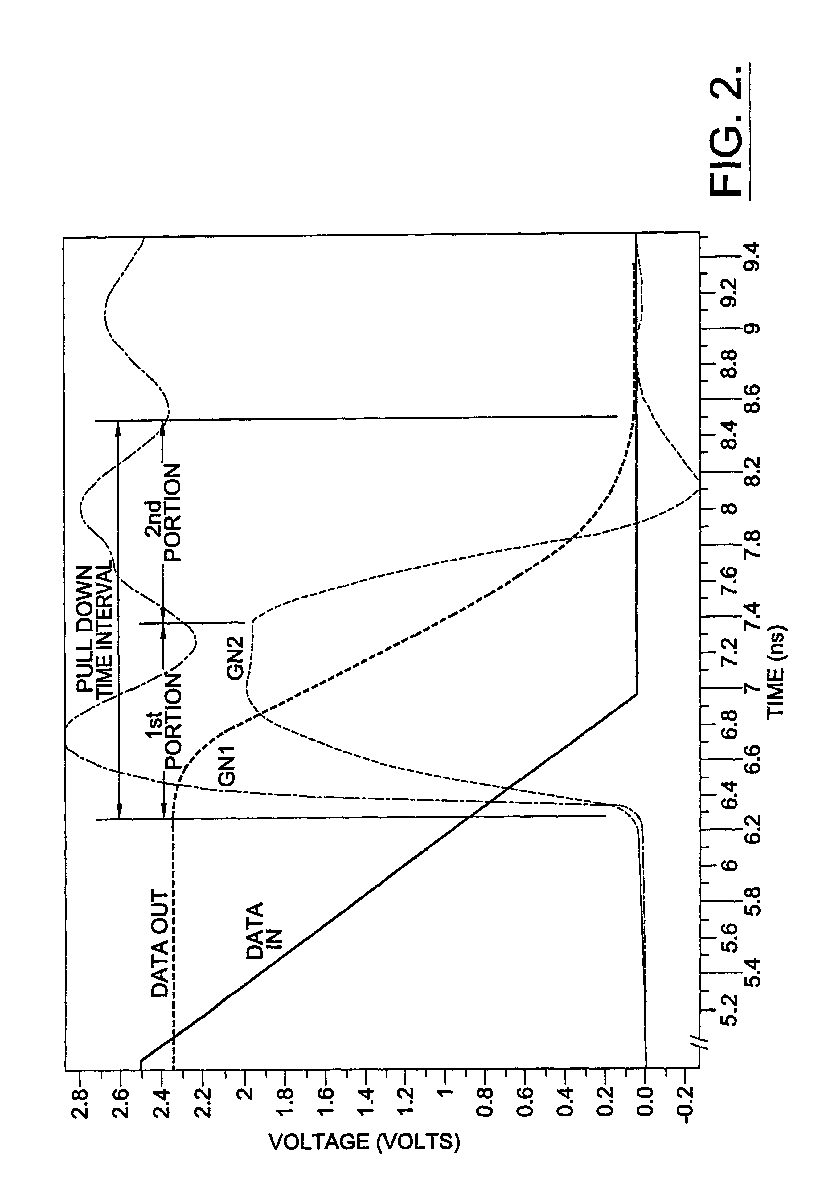
Referring now to FIG. 5, an integrated circuit output buffer 30 according to the present invention will be described. In this embodiment, a pull-down circuit 32, a control circuit 34 and an output signal line (DATA OUT) are provided. As illustrated, the pull-down circuit 32 may be provided by a pair of NMOS transistors (N7 and N8) that are electrically connected in parallel and an ESD protection resistor R5 that electrically couples the drain electrodes of the pair of transistors N7 and N8 to the output signal line. The ESD protection resistor R5 may have a resistance of 10 ohms, for example. The source electrodes of the pair of transistors N7 and N8 are also electrically connected to a first reference line (e.g., Vss). The buffer 30 also includes a preferred control circuit 34 that activates the pull-down circuit 32 by turning on both the primary and secondary pull-down transistors N7 and N8 during a leading portion of a pull-down time interval, and then turning off the secondary p...


PUM


Abstract

Integrated circuit output buffers include pull-down an pull-up circuits and a control circuit that utilizes a preferred feedback circuit to facilitate a reduction in simultaneous-switching noise during pull-down and pull-up operations and also improve the impedance matching characteristics of the output buffers during DC conditions. The preferred feedback circuit also limits the degree to which external noise can influence operation of the control circuit. Each of the pull-down and pull-up circuits may comprise a respective pair of primary and secondary transistors. The pull-down circuit is preferably configured so that the primary and secondary pull-down transistors (e.g., NMOS transistors) are electrically coupled to an output signal line (through an ESD protection resistor) and a first reference signal line (e.g., Vss). The control circuit is designed to activate the pull-down circuit by turning on both the primary and secondary pull-down transistors during a leading portion of the pull-down time interval and by turning off the secondary pull-down transistor during a trailing portion of the pull-down time interval using a first feedback switch that is electrically coupled in series between the output signal line and a gate electrode of the secondary pull-down transistor so that a signal representing a potential of said output signal line can be passed through the first feedback switch to the gate electrode of the secondary pull-down transistor.

Description

The present invention relates to integrated circuit devices, and more particularly to integrated circuit output buffers.Integrated circuits typically include buffer circuits therein for driving on-chip and off-chip loads. Dynamic output control (DOC) can also be provided by output buffers, such as those disclosed in application notes by Texas Instruments, Inc. (see, http: / / www.ti.com / sc / AVC). In particular, these output buffers having DOC circuitry may provide variable output impedance to reduce signal noise during output transitions. In these buffers, the DOC circuitry is stated as providing enough current to achieve high signaling speeds, while also having the ability to quickly switch the impedance level to reduce the undershoot and overshoot noise that is often found in high-speed logic. Such DOC circuitry may be used advantageously to eliminate the need for damping resistors which can limit noise but typically also increase propagation delay.Additional buffer circuits are also ...

Claims


Application Information

Patent Timeline
Patent Type & Authority Patents(United States)
IPC IPC(8): H03K17/16
CPCH03K17/164
Inventor SHAMARAO, PRASHANT
Owner INTEGRATED DEVICE TECH INC
Why Eureka
Try Eureka