Light-emitting diode device and method of manufacturing the same

a technology of light-emitting diodes and led devices, which is applied in the direction of semiconductor/solid-state device manufacturing, semiconductor devices, electrical apparatus, etc., can solve the problems of high fabrication cost, difficult conventional manufacturing, and inability to directly form n-type electrodes on sapphire substrates

Inactive Publication Date: 2001-07-03
EPISTAR CORP
View PDF8 Cites 143 Cited by
  • Summary
  • Abstract
  • Description
  • Claims
  • Application Information

AI Technical Summary

Problems solved by technology

Consequently, it is impossible to directly form the n-type electrode on the sapphire substrate.
As a result of the two-wire-bonding characteristic, the complication of the conventional process of manufacturing the blue LED and the die size of the blue LED are both greatly increased, which result in a high fabrication cost.
Therefore, it is very difficult for the conventional blue LED to achieve a uniform A current spreading

Method used


Image

  • Light-emitting diode device and method of manufacturing the same
  • Light-emitting diode device and method of manufacturing the same
  • Light-emitting diode device and method of manufacturing the same

Examples


first embodiment

[First Embodiment]

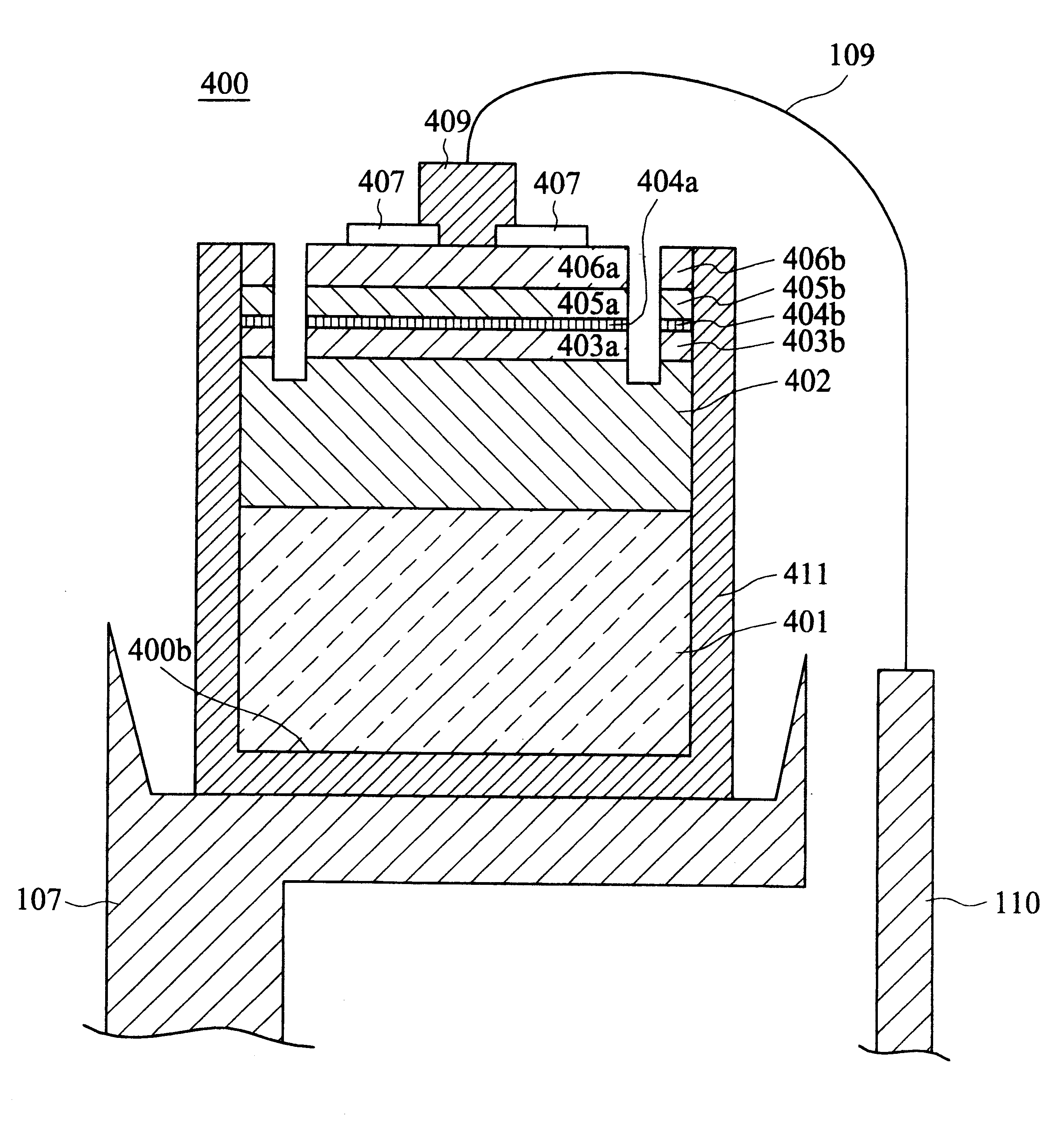
FIGS. 4(a) to 4(e) are cross-sectional views showing the steps of manufacturing a blue LED 400 according to a first embodiment of the present invention.

Referring to FIG. 4(a), an n-type layer 402 with a thickness of 3 .mu.m to 5 .mu.m is first formed on an insulating substrate 401. The insulating substrate 401 is usually made of sapphire. On the n-type layer 402, an n-type confining layer 403 with a thickness 0.1 .mu.m to 0.3 .mu.m, an active layer 404 with a thickness of 500 .ANG. to 2000 .ANG. for emitting the light, a p-type confining layer 405 with a thickness of 0.1 .mu.m to 0.3 .mu.m, and a p-type layer 406 with a thickness of 0.2 .mu.m to 1 .mu.m are sequentially formed. Each of these layers 402 to 406 is made of a GaN-based compound semiconductor material. For example, a quaternary compound semiconductor material of In.sub.x Al.sub.y Ga.sub.1-x-y N can be adopted to form the layers 402 to 406 with different conductivity types and concentrations of dopants, ...

second embodiment

[Second Embodiment]

FIG. 7 is a cross-sectional view showing a blue LED 700 according to a second embodiment of the present invention. In FIG. 7, the elements of the blue LED 700 similar to that of the blue LED 400 shown in FIGS. 4(a) to 4(e) are referred to as the similar reference numerals. For the sake of simplification, only the difference of the second embodiment from the first embodiment is described hereinafter.

During manufacturing of the blue LED 700, all steps are the same as that of manufacturing the blue LED 400 shown in FIGS. 4(a) to 4(e) except for an adhesion layer 701 is formed to cover the sidewalls 400a and the bottom surface 400b of the LED structure 700 before the formation of the conductive layer 411. The adhesion layer 701 is used to enhance the adhesive property between the sidewalls and bottom surface of the insulating substrate 401 and the conductive layer 411. The material of the adhesion layer 701 may be Ti, Ni, Al, Cr, Pd, or any metal which can enhance the...

third embodiment

[Third Embodiment]

FIG. 8 is a cross-sectional view showing a blue LED 800 according to a third embodiment of the present invention. In FIG. 8, the elements of the blue LED 800 similar to that of the blue LED 400 shown in FIGS. 4(a) to 4(e) are referred to as the similar reference numerals. For the sake of simplification, only the difference of the third embodiment from the first or second embodiment is described hereinafter.

As described in the first and second embodiment, the light generated in the central active layer 404a is then emitted out of the blue LED 400 through the top side, i.e. the central p-type layer 406a, of the blue LED 400. However, the third embodiment provides a blue LED 800 which emits out the light generated in the central active layer 404a through the bottom side, i.e. the insulating substrate 401, of the blue LED 800.

In order to achieve the blue LED 800 of the third embodiment, the conductive layer 801 is formed as a light-transmissive layer to allow the trans...


PUM


Abstract

A light-emitting diode device, such as a blue, green, blue-green light-emitting diode, with a one-wire-bonding characteristic and the method of manufacturing the same have been disclosed. The light-emitting diode device has a GaN-based semiconductor laminated structure formed on an insulating substrate. The GaN-based semiconductor laminated structure includes an n-type layer on its bottom side, a p-type layer on its top side, and an active layer, for generating light, sandwiched between the n-type and p-type layers. An annular isolation portion such as a trench or a high resistivity portion formed by ion implantation is formed in the GaN-based semiconductor laminated structure to separate the p-type layer into a central p-type layer and a peripheral p-type layer and to separate the active layer into a central active layer and a peripheral active layer. A p-type electrode is formed on the central p-type layer without electrically connecting to the peripheral p-type layer. A conductive layer is coated to cover the sidewalls and the bottom surface of the insulating substrate and to ohmically contact with the n-type layer. Preferably, an adhesion layer is sandwiched between the sidewalls and the bottom surface of the insulating substrate and the conductive layer to enhance the adhesive property. According to the present invention, the conductive layer may be formed as a mirror-like reflector or a light-transmissive layer.

Description

A. Field of the InventionThe present invention relates to a light-emitting diode (LED) device and the method of manufacturing the same. More particularly, the present invention relates to an LED device, made of GaN-based compound semiconductor materials, whose sidewalls and bottom surface are both covered with a conductive layer, and the method of manufacturing the same.B. Description of the Related ArtIn recent years, the GaN-based compound semiconductor has received more and more attention to use of a material for manufacturing blue, green, blue-green light-emitting devices, such as blue LEDs or blue laser diodes (LDs). The blue LED, for example, generally has a structure including at least one n-type GaN-based compound semiconductor layer, an active layer made of an intrinsic or doped GaN-based compound semiconductor material, and at least one p-type GaN-based compound semiconductor layer, which are sequentially laminated on a substrate.In manufacturing the conventional blue LED,...

Claims


Application Information

Patent Timeline
IPC IPC(8): H01L33/00H01L33/20H01L33/32H01L33/40H01L33/46
CPCH01L33/20H01L33/405H01L33/46H01L33/32H01L2224/32245H01L2224/48091H01L2224/48247H01L2224/73265H01L2224/48257H01L2224/48465H01L2224/49107H01L2924/00014H01L2924/00
Inventor LIN, MING-DER
Owner EPISTAR CORP
Why Eureka
Try Eureka