Method and apparatus for semiconductor processing chamber pressure control

a technology of pressure control and semiconductors, applied in the direction of coatings, metallic material coating processes, chemical vapor deposition coatings, etc., can solve the problems of large volume of pressure control volume, delay in chamber pressure change, and long resonance time of gases within the chamber

Inactive Publication Date: 2001-07-17
APPLIED MATERIALS INC
View PDF1 Cites 145 Cited by
  • Summary
  • Abstract
  • Description
  • Claims
  • Application Information

AI Technical Summary

Problems solved by technology

Although pressure control using the system described above has proven to be robust, the large size of the pressure control volume delays changes in chamber pressure in response to pressure control measures (i.e., such as throttle valve actuation).
Additionally, since the pressure control volume is substantially equal to the chamber volume, the resonance time of gases within the chamber is long.
Long resonance times of etchants result in other components within the chamber having to be replaced frequently (i.e., high cost of consumables) while long resonance times of reaction by-products may contribute to chamber and wafer contamination.
Moreover, large volumes generally require more gases to obtain desired process concentrations, longer purge times, and greater processing cost.

Method used


Image

  • Method and apparatus for semiconductor processing chamber pressure control
  • Method and apparatus for semiconductor processing chamber pressure control
  • Method and apparatus for semiconductor processing chamber pressure control

Examples


Embodiment Construction

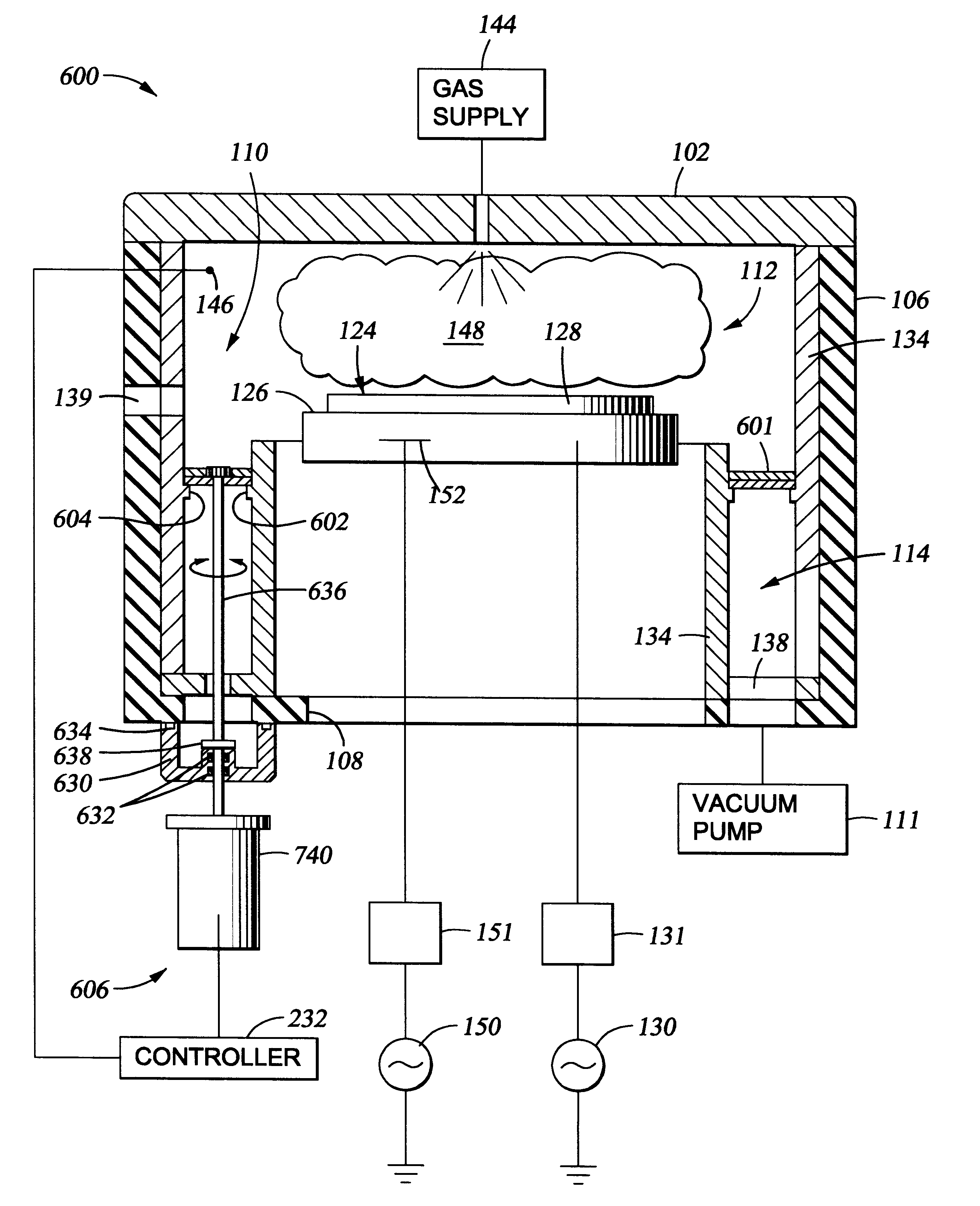
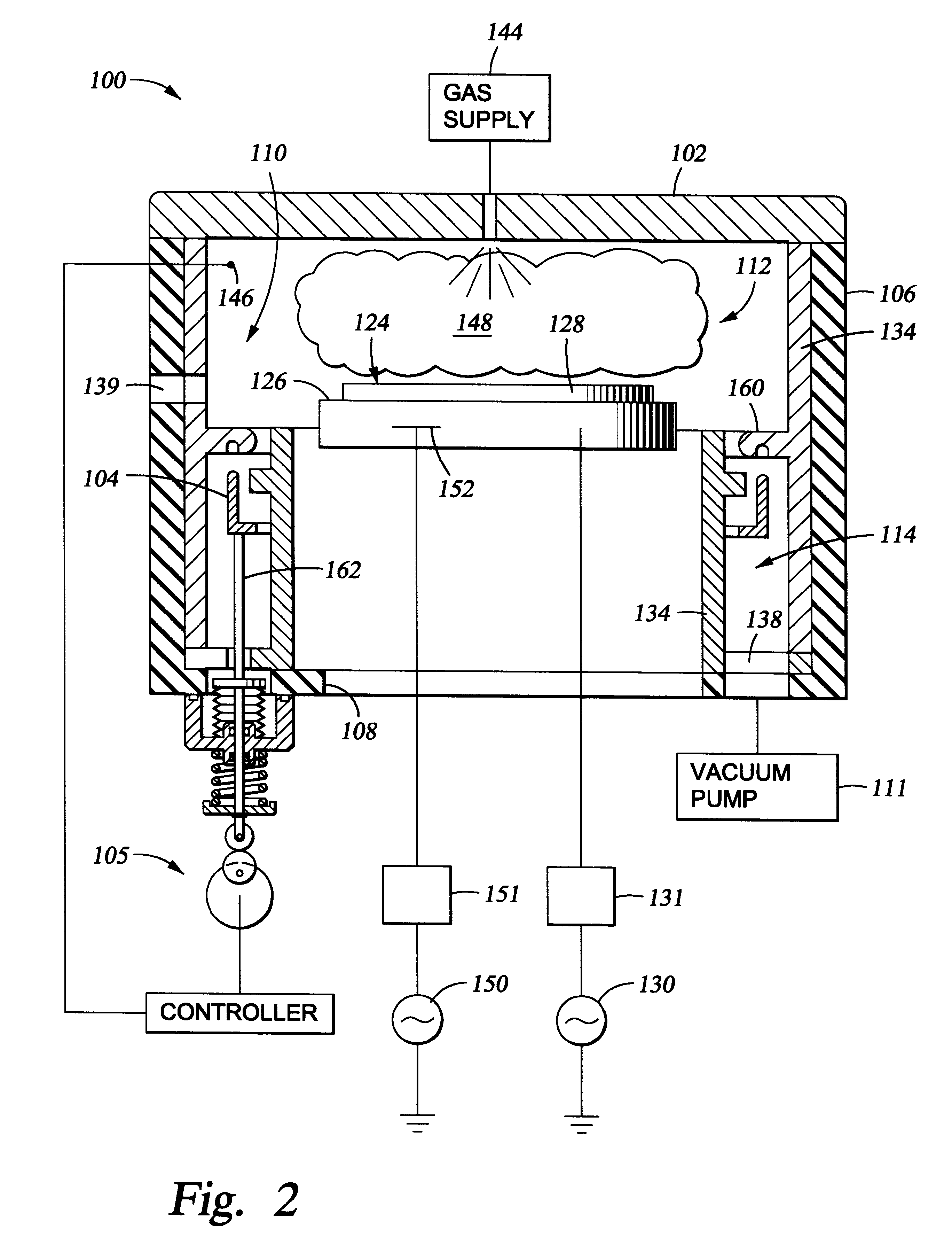
The present invention generally provides an apparatus for controlling chamber pressure within a semiconductor substrate processing system. The invention is illustratively described below as an etch chamber. However, it should be understood that the description applies to other chamber configurations such as physical vapor deposition chambers, chemical vapor deposition chambers and any other chamber in which control of pressure within a chamber is desired.

FIG. 2 is a cross sectional view of one embodiment of an etch chamber 100 of the present invention having a pressure control ring 104 configured as a parallel plate etch reactor. However, other chambers and configurations are contemplated by the inventor. Generally, the pressure control ring 104 is movably connected to a ring actuator 105, preferably residing outside of the chamber 100.

The chamber 100 generally includes an annular sidewall 106, a bottom wall 108, and a lid 102 that define a chamber volume 110. Generally, the chamber...


PUM

PropertyMeasurementUnit
pressureaaaaaaaaaa
volumeaaaaaaaaaa
biasing forceaaaaaaaaaa

Abstract

A pressure controlled substrate processing chamber comprising a pressure control ring and a throttling ridge. The pressure control ring is movably disposed proximate the throttling ridge to define a variable flow orifice. The pressure control ring is translated by a ring actuator in response to pressure information retrieved from the processing chamber. The translation of the pressure control ring causes the size of the orifice to change, thus inducing a pressure change within the chamber.

Description

BACKGROUND OF THE DISCLOSURE1. Field of InventionThe present invention relates generally to a semiconductor substrate processing apparatus. More specifically, the invention relates to an apparatus and method for providing pressure control within a semiconductor processing chamber.2. Background of the InventionIn plasma processing of semiconductor substrates, certain processing steps require the regulation of chamber pressures and removal of gases and process residues from a processing chamber. Typically, pressure regulation and the removal of such gases and process residues are facilitated through the use of a vacuum pump and throttle valve coupled to an exhaust port of the processing chamber.FIG. 1 depicts an exemplary semiconductor substrate processing system 10 having a throttle valve 38 and vacuum pump 40. An example of such a chamber is described by Collins in U.S. Pat. No. 5,707,486, issued Jan. 13, 1998.The processing system 10 comprises a process chamber 44 having a bottom 2...

Claims


Application Information

Patent Timeline
Patent Type & Authority Patents(United States)
IPC IPC(8): C23C16/44H01L21/00C23C16/455
CPCC23C16/4412H01L21/67017C23C16/45591C23C16/45557
Inventor SCHNEIDER, GERHARDNGUYEN, ANDREW
Owner APPLIED MATERIALS INC
Why Eureka
Try Eureka