Dynamic termination logic driver with improved impedance control

a technology of impedance control and driver, applied in the direction of pulse technique, oscillation generator, reliability increasing modifications, etc., can solve the problems of limiting the overall system performance, and affecting the settling time of the signal

Inactive Publication Date: 2002-07-16
ORACLE INT CORP
View PDF43 Cites 60 Cited by
  • Summary
  • Abstract
  • Description
  • Claims
  • Application Information

AI Technical Summary

Problems solved by technology

The signal frequency at which this communication occurs can limit the performance of the overall system.
Ringing due to reflections from impedance mismatches within the bus system is another factor which affects the settling time of the signal.
The effectiveness of the termination of the bus is another factor which affects the settling time of the signal.
Having high crowbar current may cause the driver to consume more power than necessary to provide adequate driver performance.
There are significant design differences between HSTL driver systems and DTL driver systems.
The brief changes, in turn, can produce undesirable voltage-spike "glitches" in the output of the driver 110.
Therefore, the fall turning on of PFET's 1500 is very slow.
For drivers consisting of transistors, establishing and maintaining a desired output impedance is problematic.
Although each bit of the pull up circuit 202 achieves impedance linearization by connecting a PFET transistor in parallel with an NMOS transistor, it would be impractical to use a P channel device in the output element of the pull down circuit 204 as the width of the P channel device would have to be very large.
Thus, the lack of tight control has little effect on overall driver 110 functioning.
Therefore, too-rapid a turning-off of the pull down circuit 204 could produce a very large "di / dt", and therefore, a large ground bounce.

Method used


Image

  • Dynamic termination logic driver with improved impedance control
  • Dynamic termination logic driver with improved impedance control
  • Dynamic termination logic driver with improved impedance control

Examples


Embodiment Construction

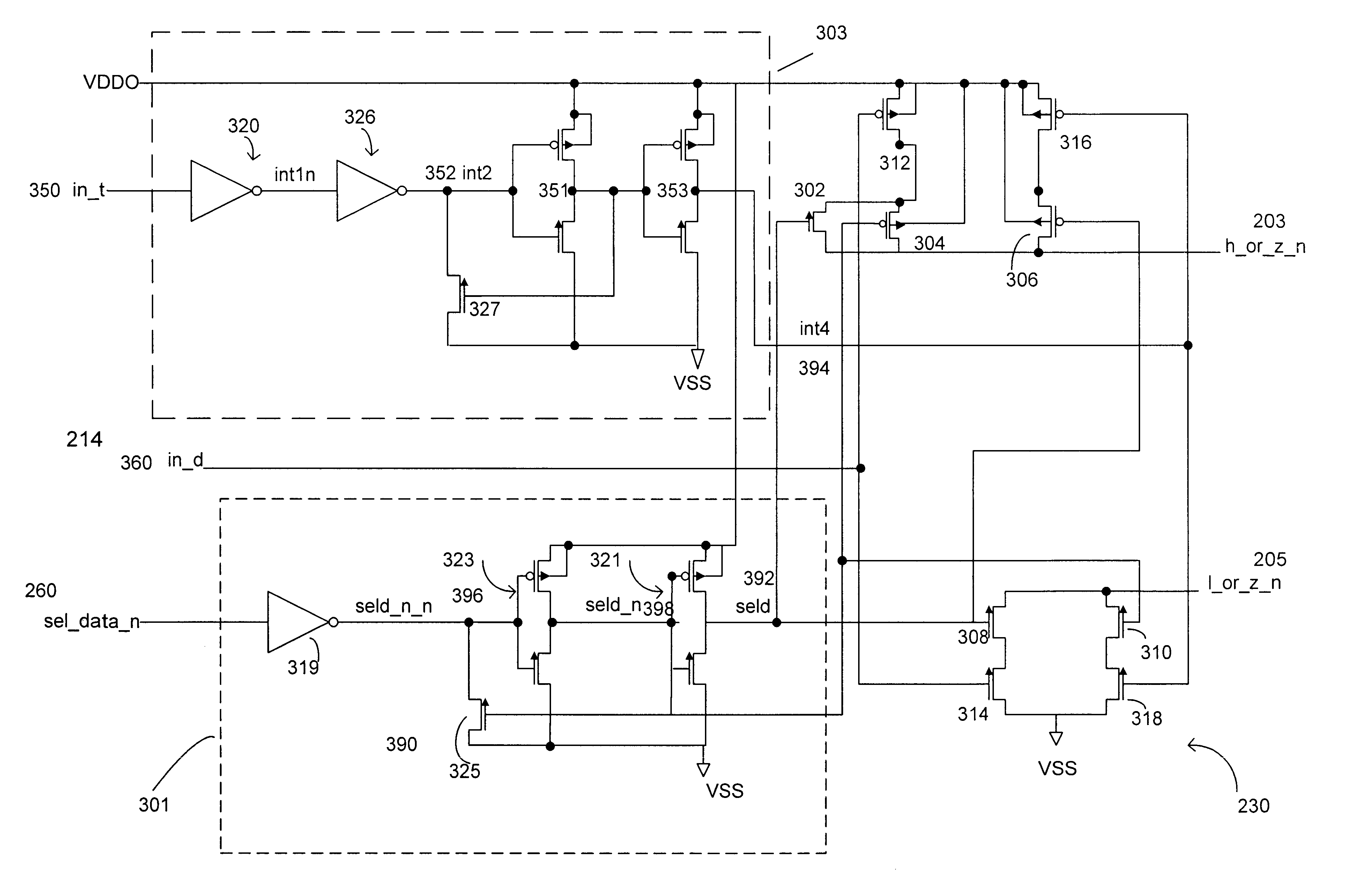
Other embodiments are within the following claims. For example, one of ordinary skill in the art appreciates that the stated limits are approximations and a function of tolerances in power supply variation, in the number of supplemental bits employed, and a host of other factors affecting that the driver herein disclosed. Further, one of ordinary skill in the art will appreciate that the driver circuitry may be implemented in a complementary fashion whereby N-channel transistors are replaced with P-channel transistors and vice versa, where appropriate.

Additionally, the driver alternatively includes either or both slew rate control circuitry and impedance control circuitry within the driver.

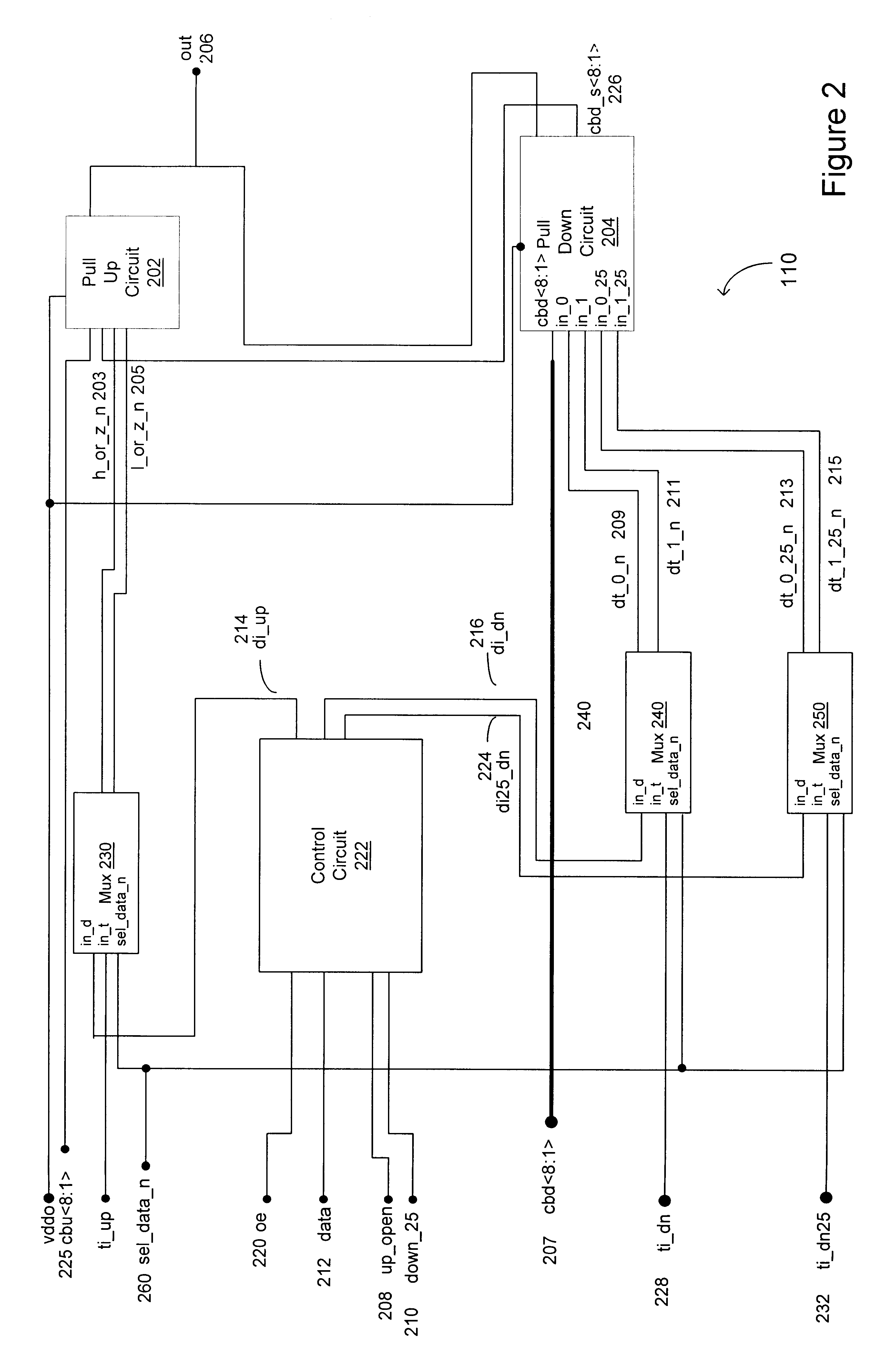
Additionally, one skilled in the art appreciates that components within both the pull up circuit 202 and the pull down circuit 204 may optionally be represented by multiplexors. In one embodiment, for example, pull up circuit 202 and pull down circuit 204 are represented by multiplexors wherein a ...


PUM


Abstract

A driver capable of launching signals into a transmission line and of terminating signals at a receiver end of the transmission line includes within the driver a circuit for controlling the output impedance and a circuit for controlling the output slew rate. Accordingly, a desired output impedance can be advantageously established and maintained over a wide range of variations in operating conditions, manufacturing processes and output voltage levels. Such a driver also advantageously limits any crowbar current, thereby reducing the overall power consumption of the driver with little, if any, degradation of driver performance. The driver includes a pull up circuit coupled to receive at least one of a plurality of control codes. The pull up circuit includes pull up output circuit and an impedance control buffer circuit, a parallel pull up circuit, the parallel pull up circuit and the pull up output circuit being controllable to adjust the impedance of the pull up circuit. The driver also includes a pull down circuit coupled to receive at least one of the plurality of control codes. The pull down circuit includes at least one pull down output circuit and a parallel pull down circuit, the parallel pull down circuit being controllable to adjust the impedance of the pull down circuit. The output impedance of the driver is further controlled during transitional phases of turning on and turning off the pull down circuit and the pull up circuit under a plurality of process, voltage and temperature (PVT) conditions.

Description

1. Field of the InventionThe present invention relates to driver circuits and more particularly to driver circuits for use in information processing systems.2. Description of the Related ArtIn computer and information processing systems, various integrated circuit chips must communicate digitally with each other over common buses. The signal frequency at which this communication occurs can limit the performance of the overall system. Thus, the higher the communication frequency, the better. The maximum frequency at which a system communicates is a function not only of the time that it takes for the electromagnetic wavefronts to propagate on the bus from one chip to another, but also of the time required for the signals to settle to levels that can be reliably recognized at the receiving bus nodes as being HIGH or LOW, referred to as the settling time.There are several factors which affect the settling time of a signal. For example, the "slew rate" of the launched signal, i.e., the r...

Claims


Application Information

Patent Timeline
Patent Type & Authority Patents(United States)
IPC IPC(8): H03K19/003
CPCH03K19/00384
Inventor ANG, MICHAEL A.TAYLOR, ALEXANDER D.STARR, JONATHAN E.VISHWANTHAIAH, SAI V.
Owner ORACLE INT CORP
Why Eureka
Try Eureka