Target locking system for electron beam lithography

a technology of electron beam and target locking, which is applied in the field of particle beam lithography system, can solve the problems of e-beams exhibiting what is called drift, i.e., exhibiting increasing inaccuracy in one direction, and introducing errors by moving the stage back into position from the measurement area,

Inactive Publication Date: 2002-08-20
GLOBALFOUNDRIES INC
View PDF11 Cites 15 Cited by
  • Summary
  • Abstract
  • Description
  • Claims
  • Application Information

AI Technical Summary

Problems solved by technology

However, even if the beam is registered adequately when pattern printing begins, during the course of writing the pattern, the e-beam may exhibit what is referred to as drift, i.e., exhibiting increasing inaccuracy in one direction as time passes.
This measurement and reregistration can be time consuming.
Consequently, even after measuring and correcting errors, moving the stage back into position from the measurement area may actually introduce errors, such as from the stage slipping or from other move related stresses.
However, when throughput is a consideration, as it nearly always is, it is impractical to correct the beam registration prior to printing each field.
However, such a blanket exposure is unusable for high sensitivity resists.
While such a sophisticated method may be feasible with a Gaussian or fixed beam shape; it is highly improbable that such a method could be developed for a variable shape beam such as a described in U.S. Pat. No. 4,243,866 entitled "Method and Apparatus for Forming a Variable Size Electron Beam" to Pfeiffer et al.
However, this registration technique is limited to high transmission membranes and its resolution capability has not yet been evaluated.
Further, below the membrane, the beam diverges and scatters rapidly, which limits the usefulness of this technique.
However, refocusing the beam introduces hysteresis into a system such as that taught in Tanaka et al.
The hysteresis, itself reduces beam accuracy.

Method used


Image

  • Target locking system for electron beam lithography
  • Target locking system for electron beam lithography
  • Target locking system for electron beam lithography

Examples


Embodiment Construction

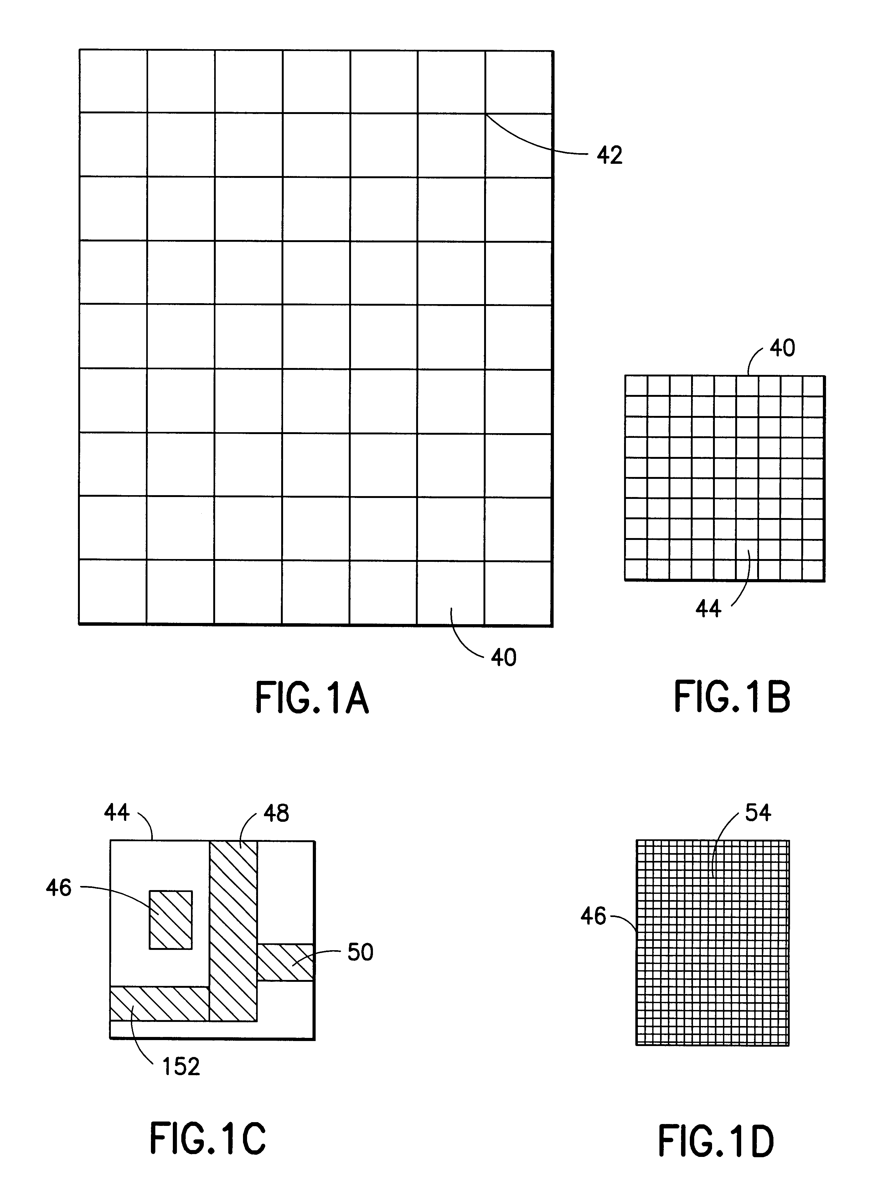
Referring now to the drawings, and more particularly, FIGS. 1A-D represent the hierarchical relationship between the individual components printed to form a pattern. FIG. 1A represents a typical substrate pattern that is divided into an array of fields 40 to accommodate a pattern which is much larger than the preferred e-beam lithography system's writing field. The collection of fields 40 is referred to as a skeleton 42. Each field 40 is identified by the x,y address of its center point. In FIG. 1B, each field 40 is divided into multiple sub-fields 44, each identified by the x, y address of its center point. In FIG. 1C, each subfield 44 may include one or more rectangles 46, 48, 50 and 52. Rectangles are logical groupings and are not specifically addressed. In FIG. 1D, each rectangle 46, 48, 50 and 52 is formed from groups of individual spots 54.

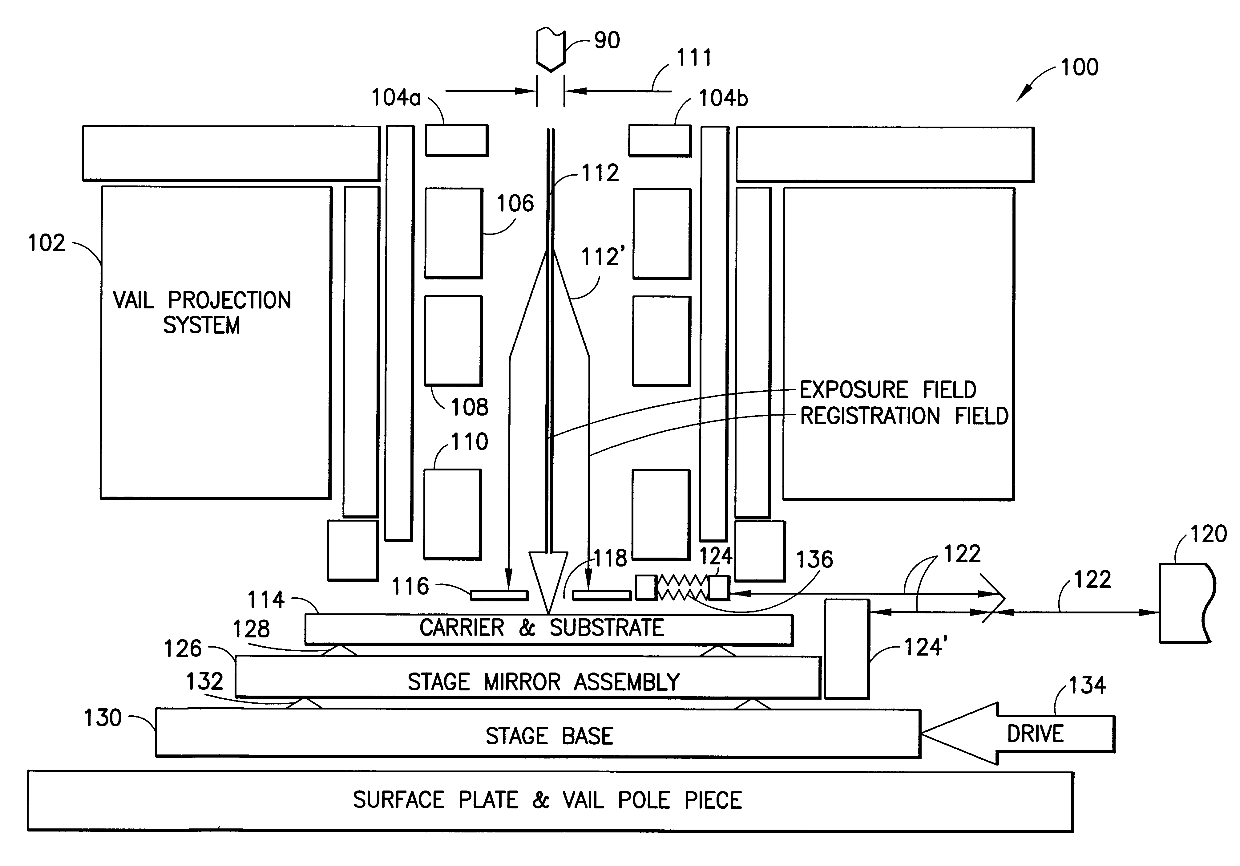
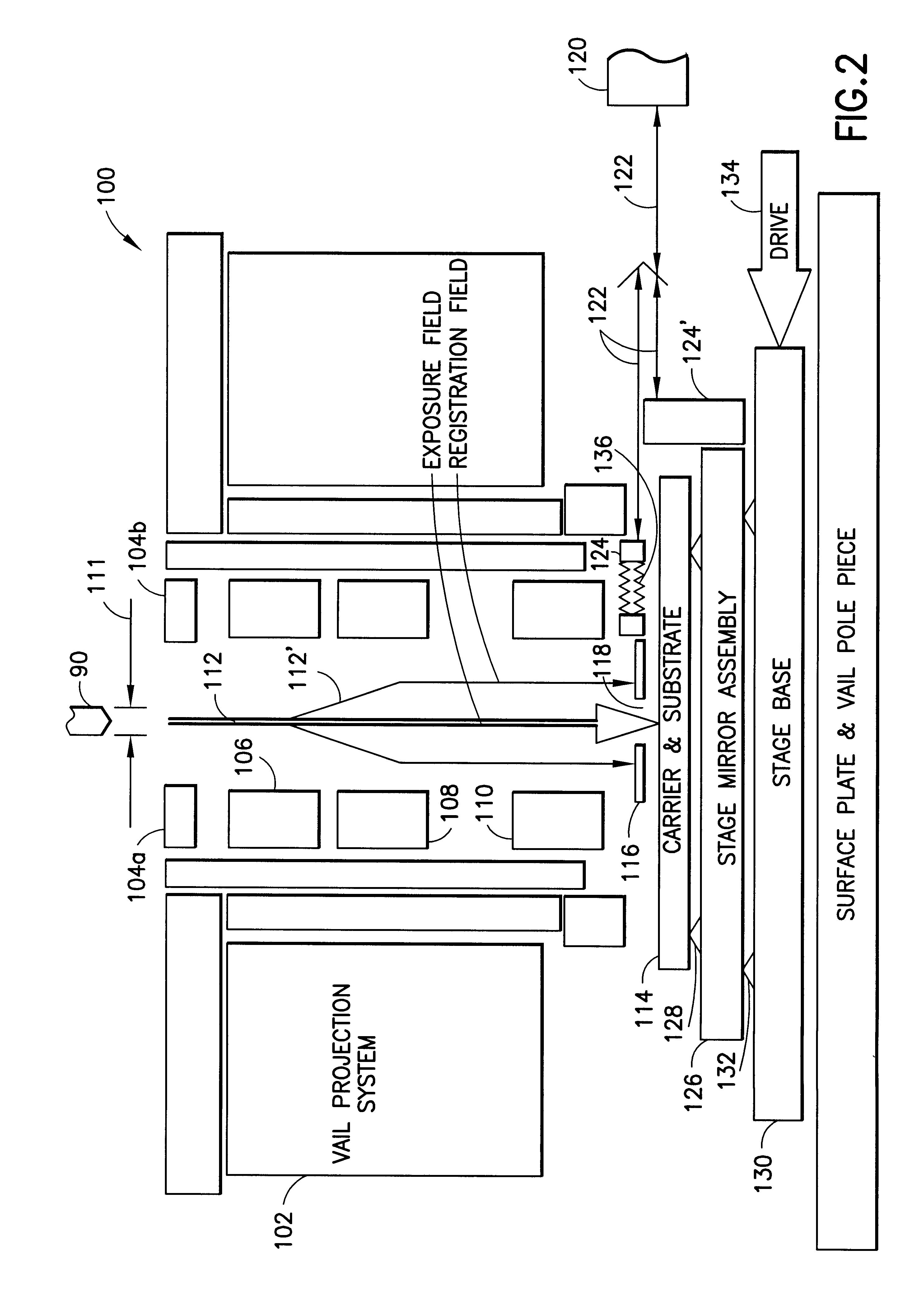
The preferred e-beam lithography system is a Variable Axis Immersion Lens (VAIL) e-beam system and is a double hierarchy deflection system....


PUM

PropertyMeasurementUnit
field sizeaaaaaaaaaa
diameteraaaaaaaaaa
distanceaaaaaaaaaa

Abstract

An e-beam lithographic system capable of in situ registration. The system has an optics section such as a VAIL lens. A controllable stage moves a substrate with respect to the beam axis to place substrate writing fields beneath the beam. A field locking target between the optics section and the stage has an aperture sized to permit the beam to write a target field on the substrate. The field locking target includes alignment or registration marks around the aperture. A differential interferometric system measures the relative positions of the field locking target and the stage and controls stage position. The beam patterns the substrate on a field by field basis. As the stage is moving into position for each field, the beam is swept until it hits the alignment marks, thereby checking system alignment. The beam control data, i.e., coil currents necessary to hit the marks are stored, and drift correction values calculated from the beam control data. Meanwhile, pattern beam control is compensated by the drift correction values.

Description

1. Field of the InventionThe present invention generally relates to particle beam lithography systems and, more particularly, to a particle beam lithography system with in situ calibration and calibration methods therefor.2. Background DescriptionElectron beam (e-beam) lithography tools are commonly used in semiconductor manufacturing to form sub-micron shapes on a semiconductor wafer. Shapes are formed by directing a beam of electrons from a source at one end of a column onto a photoresistive layer on a substrate at an opposite end of the column. A typical substrate may be 200-300 mm in diameter or larger. These submicron shapes may be formed either by writing the shape directly onto a photoresistive layer on the substrate, wherein the substrate is a semiconductor wafer; or, by writing the shape onto a photoresistive layer on a substrate which is used as a mask, subsequently, to print the shape onto the semiconductor wafer.Further, there are two broad types of writing modes used in...

Claims


Application Information

Patent Timeline
Patent Type & Authority Patents(United States)
IPC IPC(8): G01J1/00G03F7/20G03F9/02H01J37/10H01L21/02H01J37/21H01J37/304H01J37/141H01L21/027H01J37/30H01J37/02H01J37/305
CPCB82Y10/00B82Y40/00H01J37/3045H01J37/3174H01J2237/31754H01J2237/31766Y10S977/887
Inventor HARTLEY, JOHN GEORGEKENDALL, RODNEY ARTHUR
Owner GLOBALFOUNDRIES INC
Why Eureka
Try Eureka