Cap and low insertion force connector for printed circuit board

a technology of printed circuit board and connector, which is applied in the direction of coupling device connection, printed circuit aspect, coupling device details, etc., can solve the problems of reducing reducing the workability of the connection, and affecting the reliability of the connector

Inactive Publication Date: 2002-08-27
JST MFG CO LTD
View PDF6 Cites 13 Cited by
  • Summary
  • Abstract
  • Description
  • Claims
  • Application Information

AI Technical Summary

Benefits of technology

When this cap is put over the front side of the printed circuit board and the front side of the printed circuit board is inserted towards the contact, the contacting surface of the contact will be smoothly guided along the slope of the wedge-shaped cap into the window to come into contact with the conductive pad of the printed circuit board in the window. Thus, without reducing the contact force of the conductive pad of the printed circuit board and the contact, the insertion force of the printed circuit board is reduced and the connection workability is improved. Moreover, damages or the like to the contact and the conductive pad are eliminated and the reliability of the connector is enhanced. Similar effects may be obtained by chamfering the printed circuit board. Such chamfering, however, has drawbacks that the existing printed circuit boards can not be used directly, that beveling the edges of the front side of the printed circuit board may cause peeling of the conductive pad or scattering of the plated layers and, in turn, cause losses in terms of costs. In contrast to it, as the cap according to the present invention does not require any working on the printed circuit board, existing circuit boards can be used directly, and there will be no losses in terms of costs due to peeling of conductive pads and scattering of plated layers.
This low insertion force connector is mounted on a counterpart board by, for example, soldering the solder tails of the contacts onto the counterpart board. When the printed circuit board is placed on the slider and the slider is moved forward, the front side of the printed circuit board will be inserted into the contacts of the connector body. In the process, the contacting surfaces of the contacts will be guided smoothly along the slopes of the wedge-shaped guide onto the printed circuit board to contact the conductive pads. As a result, without reducing the contact forces between the conductive pads of the printed circuit board and the contacts, the insertion force of the printed circuit board can be reduced to improve the connection workability. Moreover, damages or the like to the contacts and conductive pads are eliminated, and the reliability of the connector is enhanced. When the slider is retreated, the printed circuit board will be withdrawn from the contacts. Similar effects can be obtained by chamfering the printed circuit board. This chamfering, however, has drawbacks that it can not be directly applied to the existing printed circuit boards, that beveling of the edges of the front side of the printed circuit board may cause peeling of the conductive pad and scattering of plated layers, and in turn, losses in terms of cost. In contrast to it, the low insertion force connector according to the present invention does not require working on the printed circuit boards, and the existing printed circuit boards can be used directly. Moreover, the connector is free of losses in terms of cost due to peeling of the conductive pad and scattering of plated layers.

Problems solved by technology

As a result, a large force is needed to insert the printed circuit board into the contacts and this greatly reduces the connection workability.
The edges of the printed circuit board may damage the plated layers of the contacts or deform the contacts; such damages may lower the reliability of the connector.
Furthermore, the conductive pads may be damaged.
Such problems are common to any printed circuit boards that are to be inserted into the connector, irrespective of whether semiconductor memories are mounted on the boards or not.
On the other hand, semiconductor memories show a tendency to increase their heat generation significantly.
This thermal load may cause deformation of the connector, which in turn results in loss of the engaging function of the engaging members.
Outward elastic deformation of the top ends of the arms by fingers may cause plastic deformation.
Such loss of the engaging function and deformation may cause problems of defective connection and disconnection of the printed circuit board.
Heat generation also poses a problem that it may make the operation of the semiconductor memories unstable.
Moreover, if the connector is exposed to effects of ambient electromagnetic waves or the like, the operation of the circuits may become unstable.
These problems are not limited to the connector that is used for printed circuit boards having semiconductor memories.
Such problems are common to the connector that is used for printed circuit boards having general semiconductor chips.
Such chamfering, however, has drawbacks that the existing printed circuit boards can not be used directly, that beveling the edges of the front side of the printed circuit board may cause peeling of the conductive pad or scattering of the plated layers and, in turn, cause losses in terms of costs.
This chamfering, however, has drawbacks that it can not be directly applied to the existing printed circuit boards, that beveling of the edges of the front side of the printed circuit board may cause peeling of the conductive pad and scattering of plated layers, and in turn, losses in terms of cost.

Method used


Image

  • Cap and low insertion force connector for printed circuit board
  • Cap and low insertion force connector for printed circuit board
  • Cap and low insertion force connector for printed circuit board

Examples


first embodiment

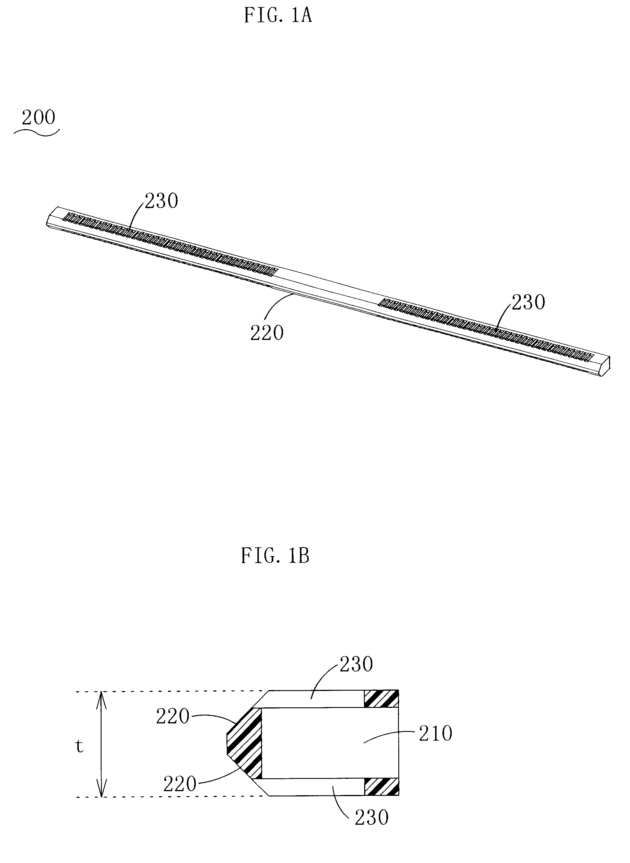
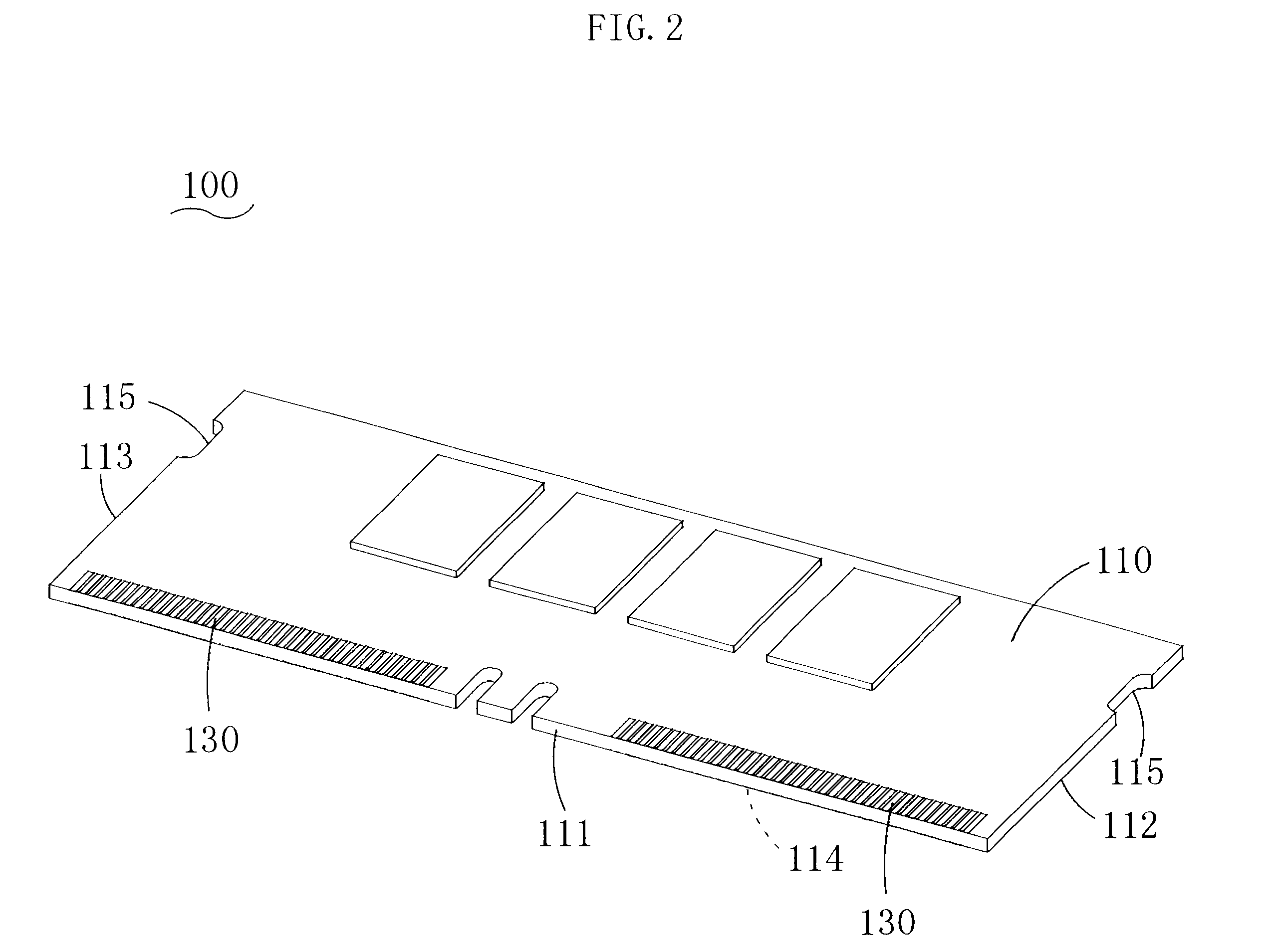
FIG. 1A through FIG. 3B show the cap. FIG. 2 shows a printed circuit board 100 that is to be connected to the connector. Conductive pads 130 being made of a conductive material are arranged on both the face and the back of the front side 111 of a rectangular board 110. In addition to this, the present invention is applicable to printed circuit boards wherein conductive pads are provided only on the face of the front side of the board and printed circuit boards wherein conductive pads are provided only on the back of the front side of the board. In this embodiment, semiconductor chips 120 are mounted on the board 110, but the present invention is also applicable to printed circuit boards wherein no semiconductor chips are mounted. If necessary, notches 115 that are concaved in the left side 112 and the right side 113 of the printed circuit board 100. For the convenience of description, the marks used for the front side, sides, bottom, etc. of the board 110 are intactly used as the ma...

second embodiment

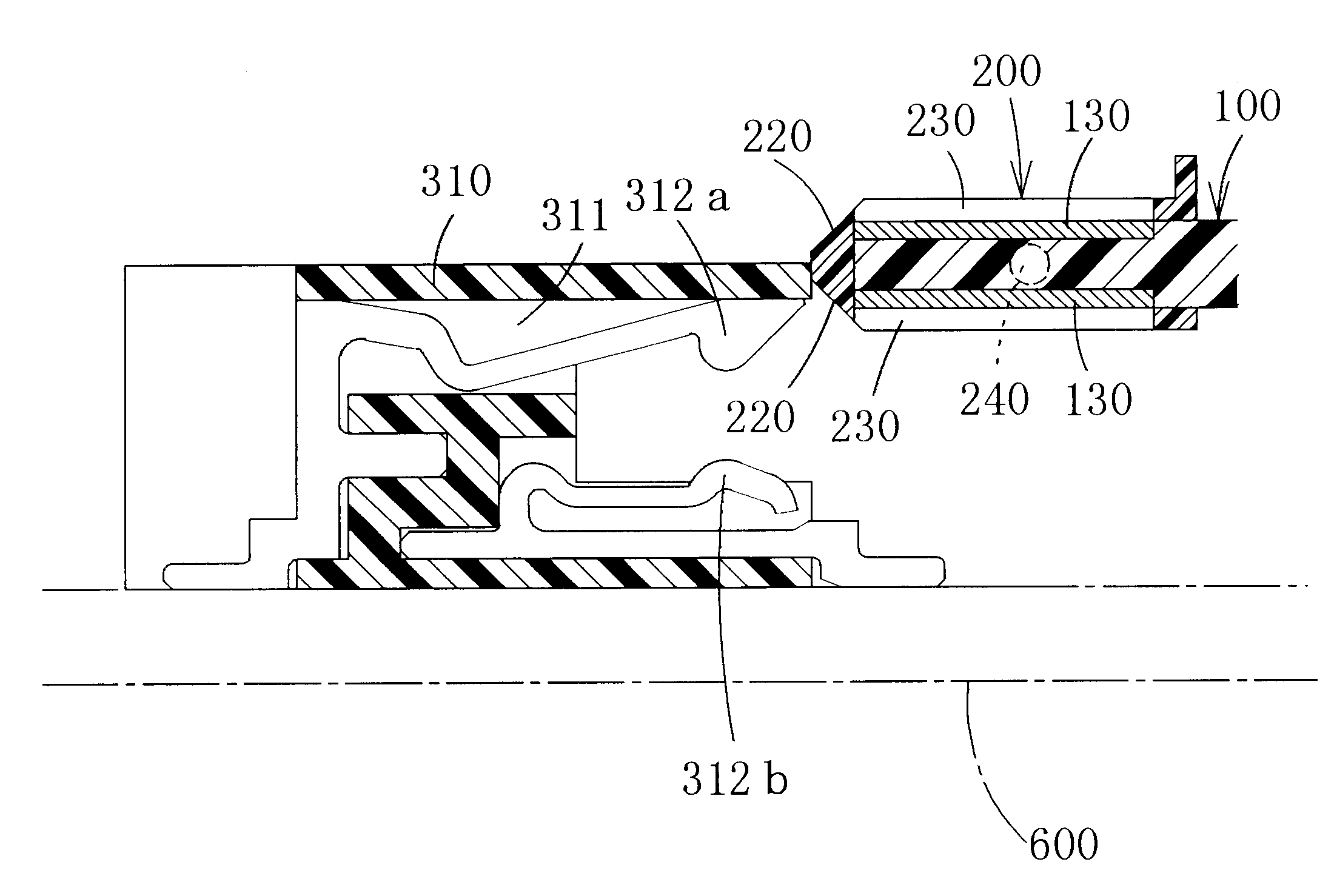
With the arrangement of the second embodiment, when the front side 111 of the printed circuit board 100 is inserted into the cap 200 being fitted to the connector 300 and the printed circuit board 100 is pushed towards the contacts 312a, 312b, the front side 111 thereof will be pushed into the contacts. When the printed circuit board 100 is pulled, the cap 200 and the printed circuit board 100 will be withdrawn from the contacts. When the printed circuit board 100 is pulled further, the printed circuit board 100 will be withdrawn from the cap 200. Thus the insertion and withdrawal of the printed circuit board 100 can be done with ease. Moreover, as the cap 200 is fitted to and is integral to the connector 300, handlability of the cap 200 is excellent.

FIG. 18 through FIG. 29B show the third embodiment being an embodiment of the connector according to the present invention. This connector 400 is to connect the printed circuit board 100 wherein, as described above, conductive pads 130 ...

third embodiment

This third embodiment or connector for printed circuit board 400 is mounted on the counterpart board 600 by, for example, soldering the solder tails of the contacts 412a, 412b onto the counterpart board 600 and, if necessary, fixing the connector body 410 onto the counterpart board 600 by means of reinforcing tabs. To fit the printed circuit board 100 into the connector 400, the printed circuit board 100 is placed on the slider 420 when the rear end of the cover 430 is up (refer to FIG. 23 through FIG. 27B), then the rear end of the cover 430 is lowered. The slider 420 will move forward and the front side 111 of the printed circuit board 100 will be inserted into the contacts 412a, 412b. When the cover 430 is put over the printed circuit board 100 and engaged to the arms 413, the printed circuit board 100 will be sandwiched by the slider 420 and the cover 430 and held in the connection position (refer to FIG. 28 through FIG. 29B). In this case, positioning of the printed circuit boa...


PUM


Abstract

A cap that is to be fitted to a printed circuit board, which has a conductive pad on the front side of the rectangular board thereof and which is to be connected to the connector. The cap is formed into a bag and is shaped into a wedge that gets thinner towards the front, and the cap has a window for exposing the conductive pad of the printed circuit board.A low insertion force connector that connects a printed circuit board having conductive pads on the front side of the rectangular board thereof. This low insertion force connector comprises a connector body having at least a pair of contacts that contact the conductive pads and clamp the printed circuit board, a slider that carries the printed circuit board and advances to and retreats from the contact, and a guide that is provided at the front end of the slider and is formed into a wedge-shape, which gets thinner towards the front.The present invention reduces the insertion force of the printed circuit board, enhances the connection workability, and eliminates damages or the like to the contacts and the conductive pad to enhance the reliability. The present invention provides a connector that is also effective in countermeasures against heat and electromagnetic waves.

Description

1. Field of the InventionThe present invention belongs to the technical field of a printed circuit board that has conductive pads on the front side of a rectangular board and a connector that connects this printed circuit board. In particular, the present invention relates to measures or the like for improving the workability of connecting the printed circuit board to the connector.2. Related ArtPrinted circuit boards of this kind include, for example, those in which semiconductor chips such as semiconductor memories are mounted on rectangular board. A connector is used extensively, which connects a printed circuit board of this kind to a printed circuit board such as a mother board (hereinafter referred to as the counterpart board) in a position wherein the two boards are approximately parallel to each other. This connector has an approximately U-shaped form to correspond to the front side, left side and right side of the printed circuit board. A groove is formed in this connector ...

Claims


Application Information

Patent Timeline
Patent Type & Authority Patents(United States)
IPC IPC(8): H01R12/16H01R12/00H05K1/11H01R13/631H01R12/83
CPCH05K1/117H01R12/83H05K2201/2027H01R12/82
Inventor YASUFUKU, KAORIHOSAKA, TAIJIMIYAZAWA, MASAAKI
Owner JST MFG CO LTD
Why Eureka
Try Eureka