Apparatus and method for electro chemical deposition

a technology of electrochemical deposition and apparatus, applied in the field of electrochemical deposition system, can solve the problems of cvd, increase the current density of the feature, and difficulty in filling structures,

Inactive Publication Date: 2002-09-24
APPLIED MATERIALS INC
View PDF8 Cites 29 Cited by
  • Summary
  • Abstract
  • Description
  • Claims
  • Application Information

AI Technical Summary

Problems solved by technology

Many traditional deposition processes, such as physical vapor deposition (PVD) and chemical vapor deposition (CVD), have difficulty filling structures where the aspect ratio exceeds 4:1, and particularly where it exceeds 10:1.
Additionally, as the feature widths decrease, the device current remains constant or increases, which results in an increased current density in the feature.
However, aluminum has a higher electrical resistivity than other more conductive metals such as copper, and aluminum also can s...

Method used


Image

  • Apparatus and method for electro chemical deposition
  • Apparatus and method for electro chemical deposition
  • Apparatus and method for electro chemical deposition

Examples


Embodiment Construction

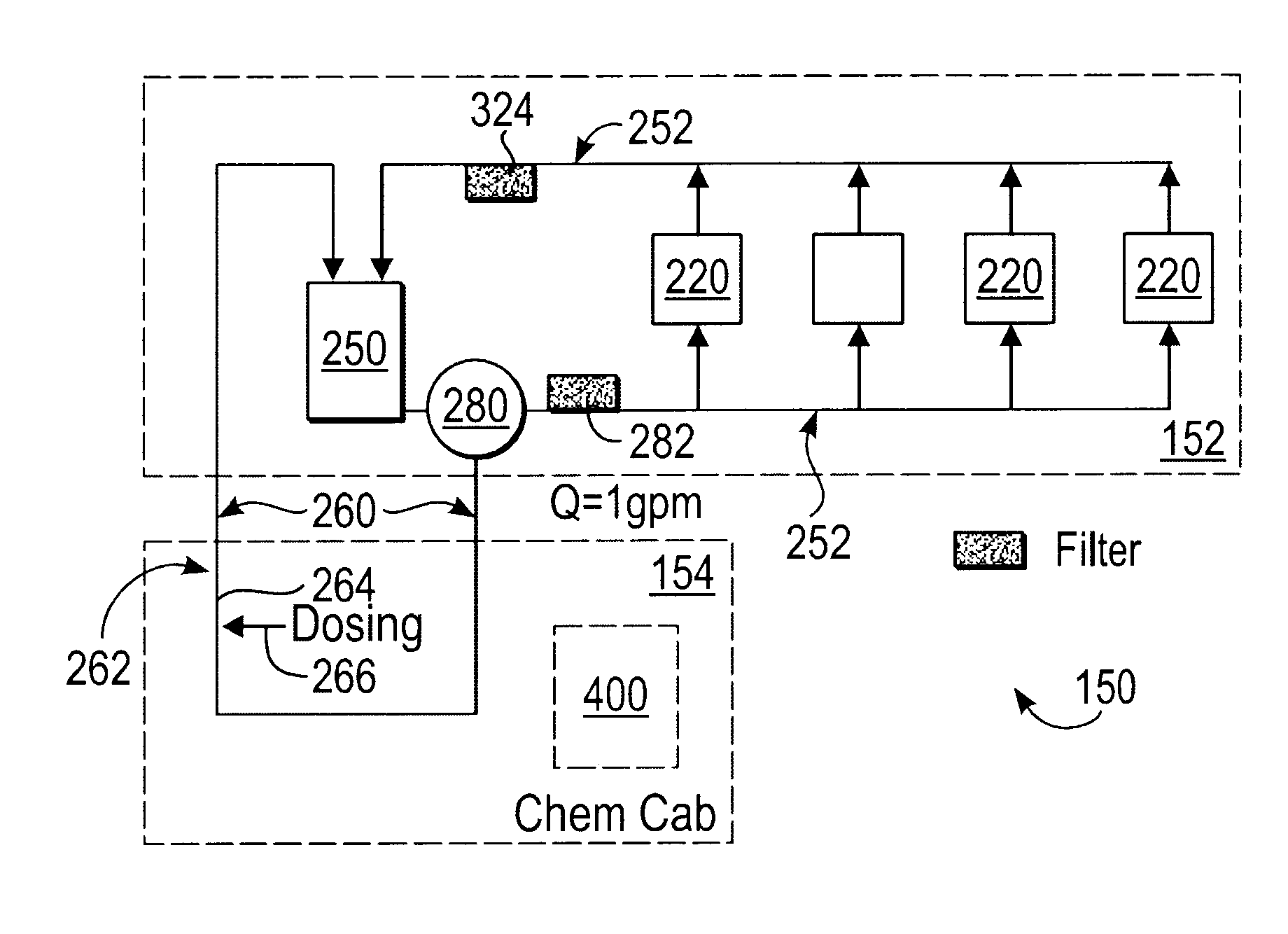
In one illustrated embodiment of the present inventions, a method and apparatus for electroplating semiconductor substrates is provided which comprises recirculating electrolyte between an electrolyte reservoir and at least one electrolytic plating cell through a reservoir-cell fluid recirculation circuit disposed in an electroplating tool platform; and recirculating electrolyte between the reservoir and a dosing unit through a reservoir-dosing unit fluid recirculation circuit which couples a dosing system platform to the electroplating tool platform. The electrolyte is dosed in the dosing system platform with additives using the dosing unit.

As explained in greater detail below, in one embodiment, the majority of the electro-chemical deposition solution, which in this embodiment is an electrolyte, recirculates locally in the electroplating tool platform. A relatively small flow of electrolyte may be diverted to the dosing system platform to be analyzed and dosed as needed. In additi...


PUM

PropertyMeasurementUnit
Lengthaaaaaaaaaa
Lengthaaaaaaaaaa
Lengthaaaaaaaaaa

Abstract

A system is provided in which a smaller flow of deposition solution is diverted from a larger flow of deposition solution flowing on an electro-chemical deposition tool platform. The smaller flow is diverted to a dosing unit which may be on a separate platform. The dosing unit in one embodiment comprises a pressurized flow line.

Description

1. Field of the InventionThe present invention generally relates to deposition of a metal layer onto a wafer or other substrate. More particularly, the present invention relates to an electro-chemical deposition system for forming a metal layer on a substrate.2. Background of the Related ArtSub-quarter micron, multi-level metallization is one of the key technologies for the next generation of ultra large scale integration (ULSI). The multilevel interconnects that lie at the heart of this technology require planarization of interconnect features formed in high aspect ratio apertures, including contacts, vias, lines and other features. Reliable formation of these interconnect features is very important to the success of ULSI and to the continued effort to increase circuit density and quality on individual substrates and die.As circuit densities increase, the widths of vias, contacts and other features, as well as the dielectric materials between them, decrease to less than 250 nanomet...

Claims


Application Information

Patent Timeline
IPC IPC(8): C25D21/14C25D21/18C25D7/12C25D21/12C25D21/00C25D17/00H01L21/288
CPCC25D21/14C25D21/18C25D17/001C25D7/123
Inventor STEVENS, JOSEPH J.RABINOVICH, YEVGENIYCHAO, SANDY S.DENOME, MARK R.D'AMBRA, ALLEN L.OLGADO, DONALD J.
Owner APPLIED MATERIALS INC
Why Eureka
Try Eureka