Imaging apparatus that starts charge accumulation in sequence based on movement speed on light-shielding member

Inactive Publication Date: 2003-04-01
NIKON CORP
View PDF12 Cites 104 Cited by
  • Summary
  • Abstract
  • Description
  • Claims
  • Application Information

AI Technical Summary

Benefits of technology

As another option, the imaging element can be an amplifying type imaging element. Ac

Problems solved by technology

At this time, when the accumulated charge is transferred from the photosensitive part A to the vertical transferring part B, it is known that there is a problem of generating smear (a phenomenon in which a vertical white line can be seen when the light intensity is strong) by leakage of charge or the like from the photosensitive part A.
However, in the case of the above-mentioned FT-CCD, the generation of smear cannot be controlled because the light can be received (by the photosensitive part A) even during the transfer of charge to the accumulation part E. In particular, the ratio between the photoelectric charge time and the signal transfer time to the accumulating part E for one level of the CCD is equal to the ratio between the signals and the smear amount.
Thus, there is a problem in that a high speed electronic shutter cannot be easily realized that sufficiently controls smear.
However, in such a structure, there is a problem of increasing the chip area.
An addi

Method used


Image

  • Imaging apparatus that starts charge accumulation in sequence based on movement speed on light-shielding member
  • Imaging apparatus that starts charge accumulation in sequence based on movement speed on light-shielding member
  • Imaging apparatus that starts charge accumulation in sequence based on movement speed on light-shielding member

Examples


Embodiment Construction

The following explains an embodiment of the present invention. However, the technical scope of the present invention is not limited to this embodiment.

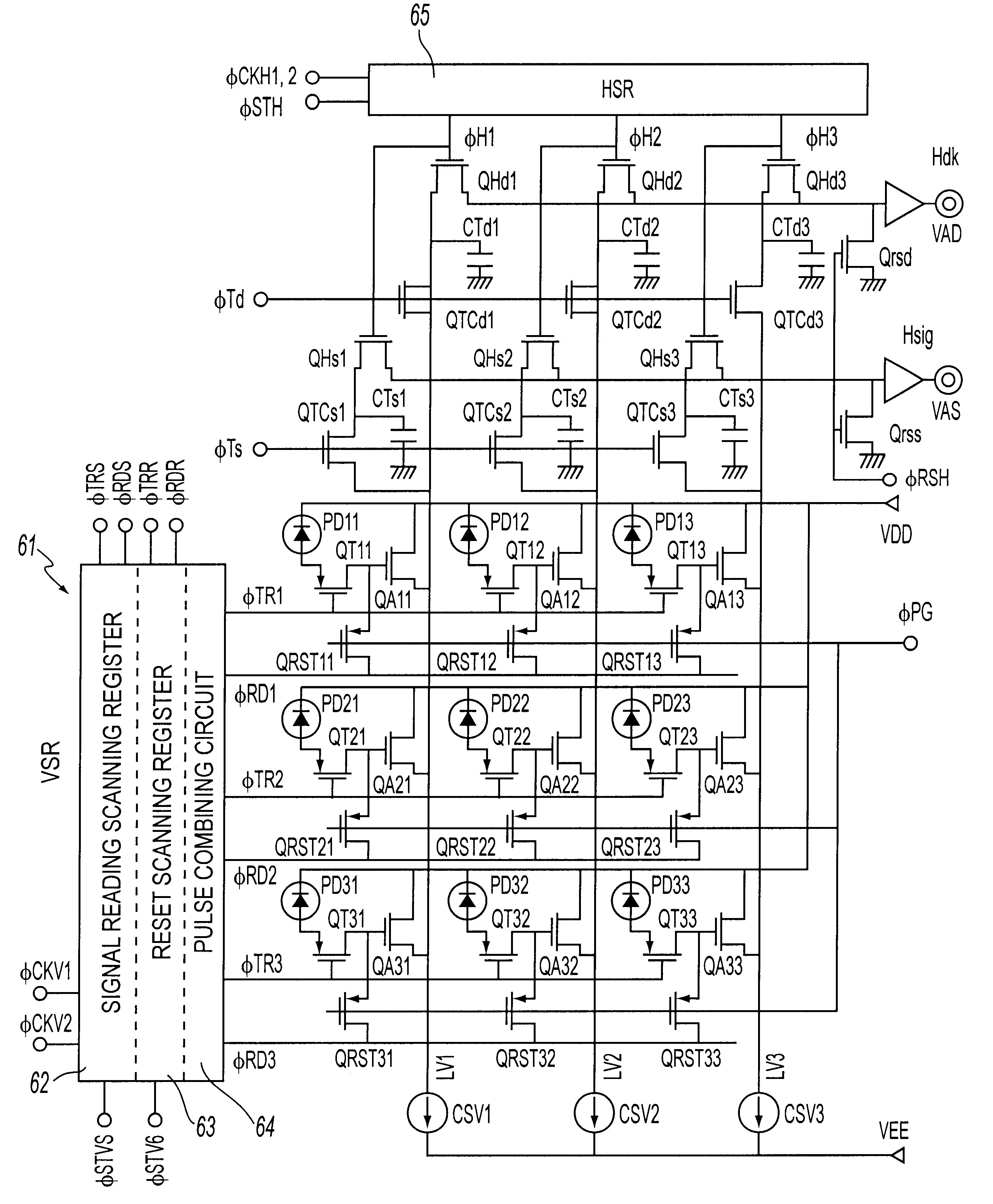
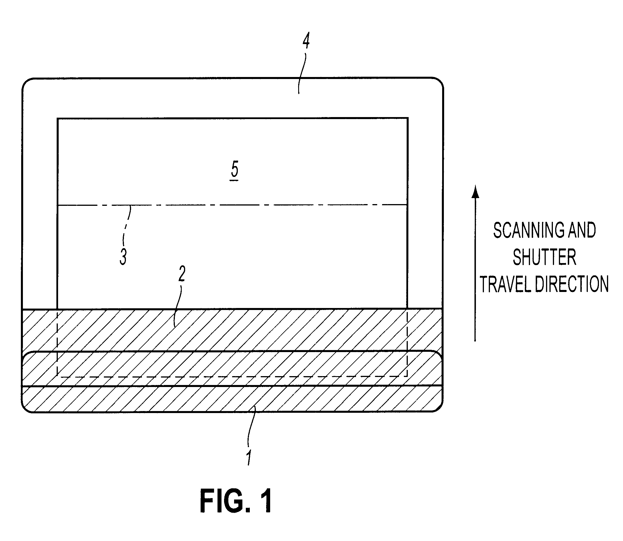
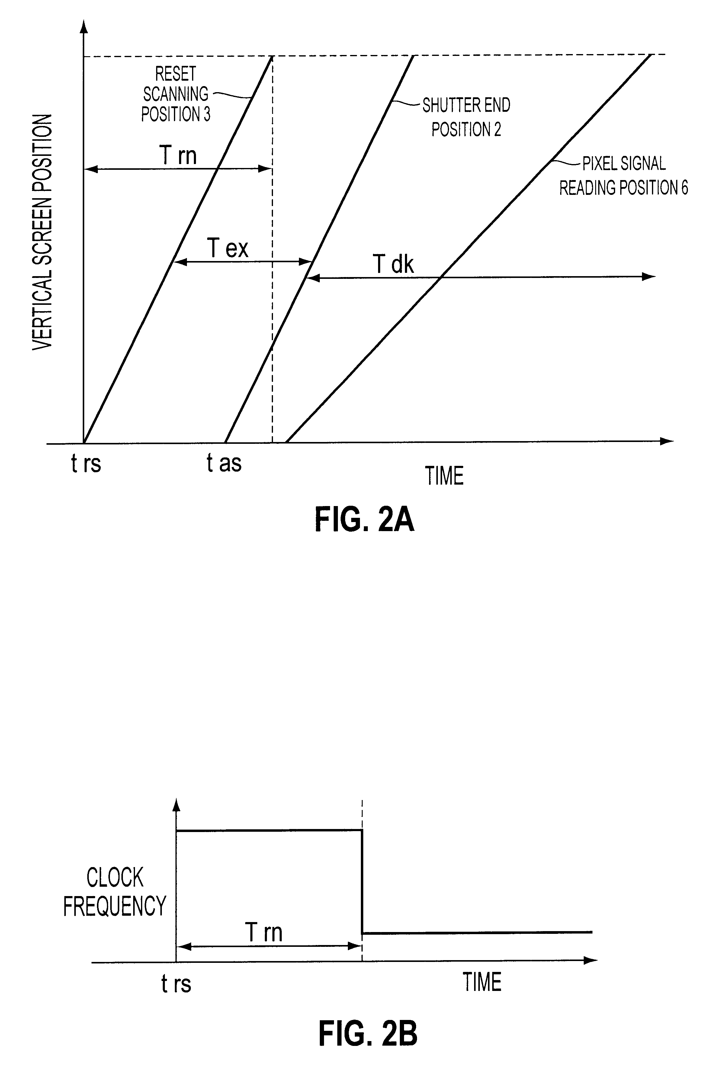
In the imaging device in the described embodiment of the present invention, an imaging element of the XY address type having a vertical scanning part and a horizontal scanning part are used. Furthermore, the vertical scanning part has a reset scanning circuit that briefly resets the accumulated charge amount of the pixels to zero, as will be described later, to perform a charge accumulation start scanning (hereafter referred to as reset scanning) in which the accumulation of the charge starts from that point (at which it was reset to zero), and a reading scanning circuit that performs a reading scanning of the charges stored by the pixels. Shooting of a moving image is performed by alternately performing the reset scanning and the reading scanning in shifted phases.

Furthermore, the imaging device in the described embodiment of the pre...


PUM


Abstract

An imaging device performs moving image shooting in which smearing does not occur and further performs a still image shooting by a sufficiently accurate shutter operation. The imaging device includes an imaging element that accumulates received light as a charge. A shutter travels so as to shade the imaging element. A first scanning circuit performs a charge accumulation start scanning of the imaging element at a timing and/or speed that matches the travel speed of the shutter. A second scanning circuit performs reading scanning of the charge accumulated in the imaging element. A controller controls the scanning of the first scanning circuit and the second scanning circuit and the travel of the shutter. When the still image is shot by the imaging device, the exposure time is adjusted by the controller controlling the scanning start time of the first scanning circuit and the travel start time of the shutter.

Description

BACKGROUND OF THE INVENTION1. Field of InventionThe present invention relates to an imaging device that shoots images using an imaging element and in which exposure is controlled by controlling an accumulation time of light received by the imaging element, and that is equipped with a shutter that shades the imaging element.2. Description of Related ArtIn an electronic camera that uses a solid-state imaging element, an electronic shutter can be used to perform exposure control by controlling the accumulation time of photoelectric charge of a photosensitive part of the imaging element. Methods of implementing this kind of electronic shutter vary depending upon the imaging element. For example, in the interline (IT) type CCD (charge coupled device) as shown in FIG. 11A, a photoelectric charge is accumulated in the photodiodes of the photosensitive part A during a specified interval and the signal charge is then transferred to a vertical transferring part B. The electronic shutter is fu...

Claims


Application Information

Patent Timeline
IPC IPC(8): H04N5/217H04N5/235H04N3/15H04N5/335H04N5/341H04N5/353H04N5/359H04N5/369H04N5/372H04N5/3745
CPCH04N5/2353H04N5/3595H04N5/3532H04N23/73H04N25/531H04N25/625
Inventor JUEN, MASAHIRO
Owner NIKON CORP
Why Eureka
Try Eureka