Multigate semiconductor device with vertical channel current and method of fabrication

a semiconductor device and vertical channel current technology, applied in semiconductor devices, digital storage, instruments, etc., can solve the problems of reducing the storage capacity of the memory and the number of devices

Inactive Publication Date: 2003-06-17
SANDISK TECH LLC
View PDF83 Cites 399 Cited by
  • Summary
  • Abstract
  • Description
  • Claims
  • Application Information

AI Technical Summary

Problems solved by technology

Unfortunately, these devices that are formed in the same plane and therefore require input / outputs (I / Os) which also run in the same plane.
Having a source and drain input / output conductors running in the same plane, significantly reduces the number of devices that can-be fabricated in a single plane and thereby significantly reduces the storage capability of the memory.

Method used


Image

  • Multigate semiconductor device with vertical channel current and method of fabrication
  • Multigate semiconductor device with vertical channel current and method of fabrication
  • Multigate semiconductor device with vertical channel current and method of fabrication

Examples


Embodiment Construction

The present invention is a novel multigate semiconductor device having vertical channel current and its method of fabrication. In the following description numerous specific details are set forth in order to provide a thorough understanding of the present invention. One of ordinary skill in the art will appreciate that these specific details are not necessary to practice the present invention. In other instances, well-known semiconductor memory layout and processing techniques have not been described in specific detail in order to not unnecessarily obscure the present invention.

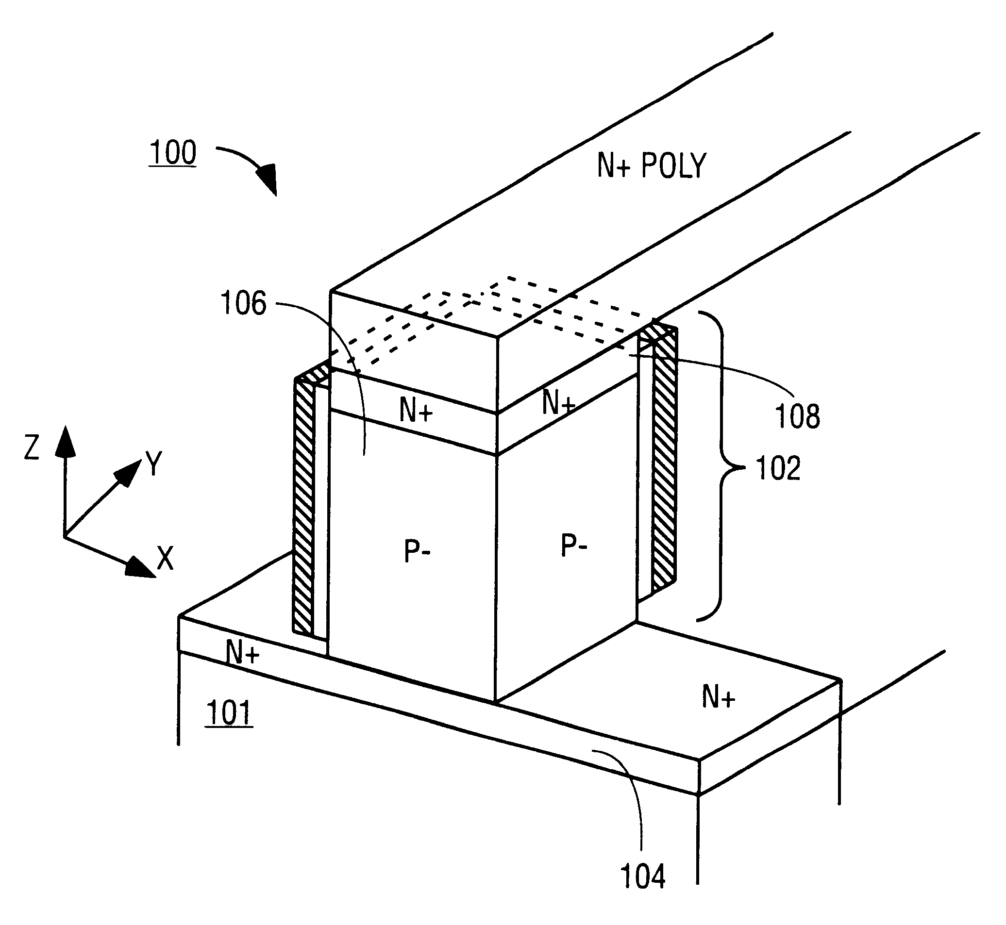
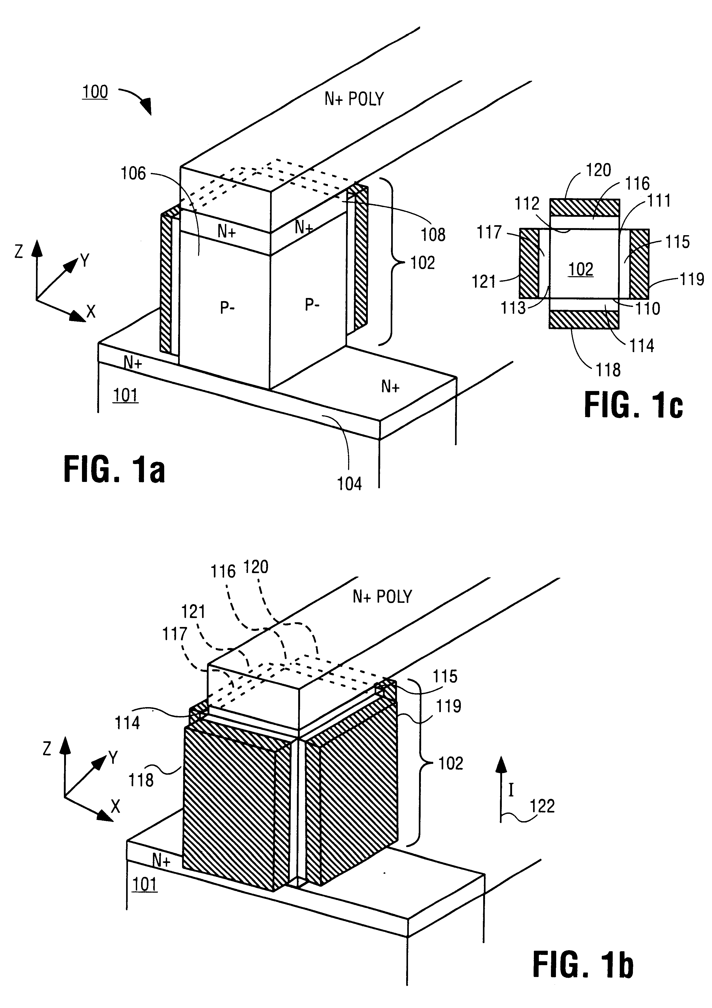
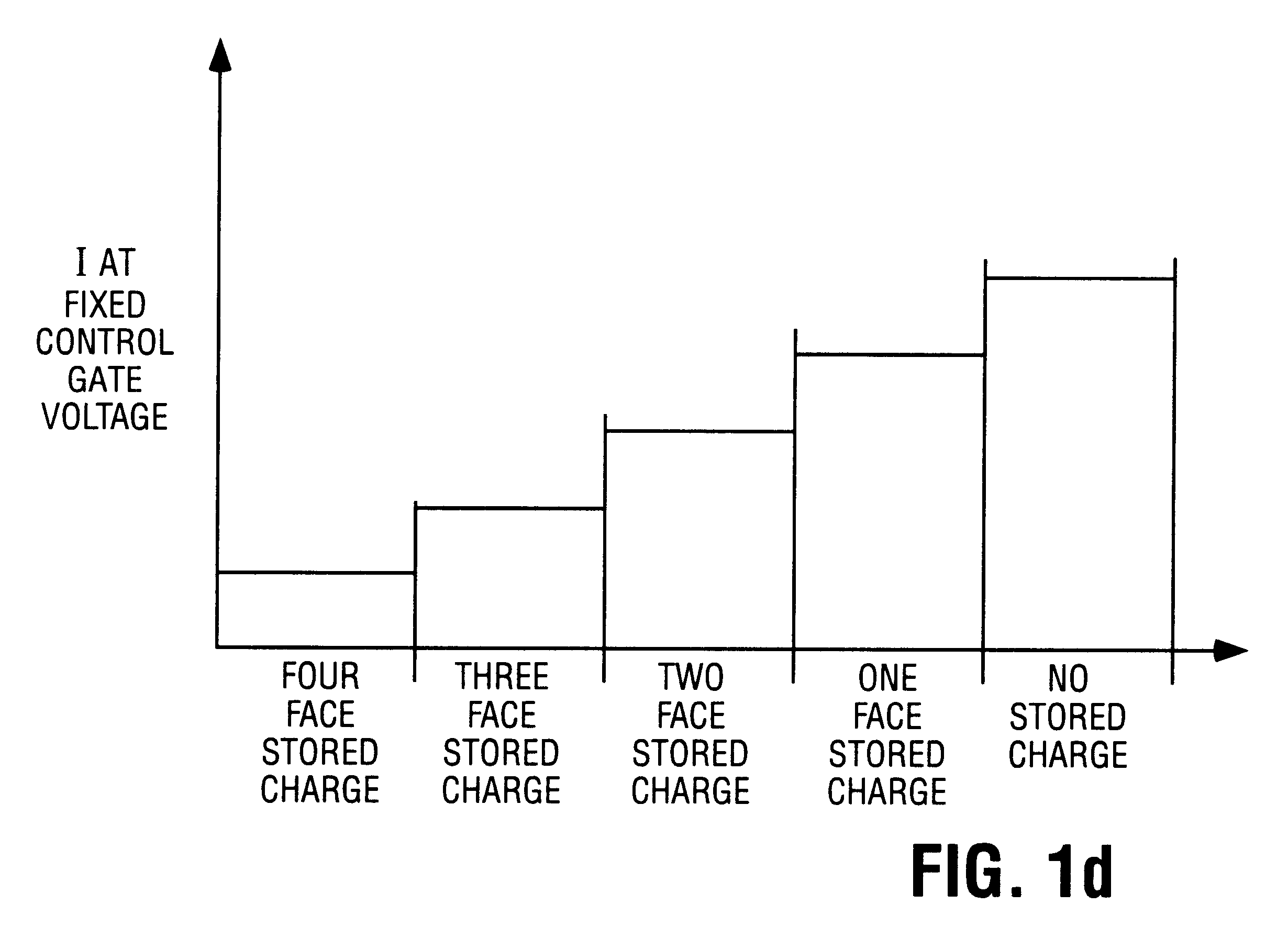
The present invention is a novel multigate semiconductor device and its method of fabrication. The multigate semiconductor device can be used as a multibit nonvolatile memory or as a multiple gate transistor. The present invention will be described with respect to a multibit nonvolatile memory. A multibit nonvolatile memory 100 in accordance with the present invention is illustrated in FIGS. 1a-1c. Nonvolatil...


PUM


Abstract

The present invention is a multibit nonvolatile memory and its method of fabrication. According to the present invention a silicon channel body having a first and second channel surface is formed. A charge storage medium is formed adjacent to the first channel surface and a second charge storage medium is formed adjacent to the second channel surface. A first control gate is formed adjacent to the first charge storage medium adjacent to the first channel surface and a second control gate is formed adjacent to the second charge storage medium adjacent to the second surface.

Description

1. Field of the InventionThe present invention relates to the field of nonvolatile memories and more specifically to a multibit nonvolatile memory and its method of fabrication.2. Discussion of Related ArtAs integrated circuits and computers have become powerful, new applications have arisen that require the ability to store large amounts of data. Certain applications require a memory with the ability to write and erase data and the ability to store data in a nonvolatile manner. Presently, such memories are formed with electrically erasable nonvolatile memories such as flash devices and EEPROMS. Unfortunately, these devices that are formed in the same plane and therefore require input / outputs (I / Os) which also run in the same plane. Having a source and drain input / output conductors running in the same plane, significantly reduces the number of devices that can-be fabricated in a single plane and thereby significantly reduces the storage capability of the memory.What is desired is a ...

Claims


Application Information

Patent Timeline
Patent Type & Authority Patents(United States)
IPC IPC(8): H01L21/70H01L21/28H01L21/02H01L21/336H01L27/115H01L29/66H01L21/3205H01L29/768H01L21/8246H01L29/76G11C11/56G11C16/04H01L21/8247H01L29/788
CPCH01L29/7881H01L21/28282H01L27/115H01L27/11556H01L27/11568H01L29/66825H01L29/66833H01L21/28273G11C11/5621G11C11/5671G11C16/0458G11C16/0475G11C2211/5611G11C2211/5612H01L29/40114H01L29/40117H10B69/00H10B41/27H10B43/30
Inventor CLEEVES, JAMES M.SUBRAMANIAN, VIVEK
Owner SANDISK TECH LLC
Why Eureka
Try Eureka