Method for forming a transistor having gate dielectric protection and structure

a gate dielectric and protection technology, applied in the direction of transistors, semiconductor devices, electrical equipment, etc., can solve the problems of reducing the life of the device, boron penetration into the gate dielectric has been a long-standing problem, and the gate side is generally the greater problem

Active Publication Date: 2009-01-29
NORTH STAR INNOVATIONS
View PDF5 Cites 77 Cited by
  • Summary
  • Abstract
  • Description
  • Claims
  • Application Information

AI Technical Summary

Problems solved by technology

Boron penetration into gate dielectrics has been a long standing problem.
The gate side has generally been the greater problem because of the rela...

Method used


Image

  • Method for forming a transistor having gate dielectric protection and structure
  • Method for forming a transistor having gate dielectric protection and structure
  • Method for forming a transistor having gate dielectric protection and structure

Examples


Embodiment Construction

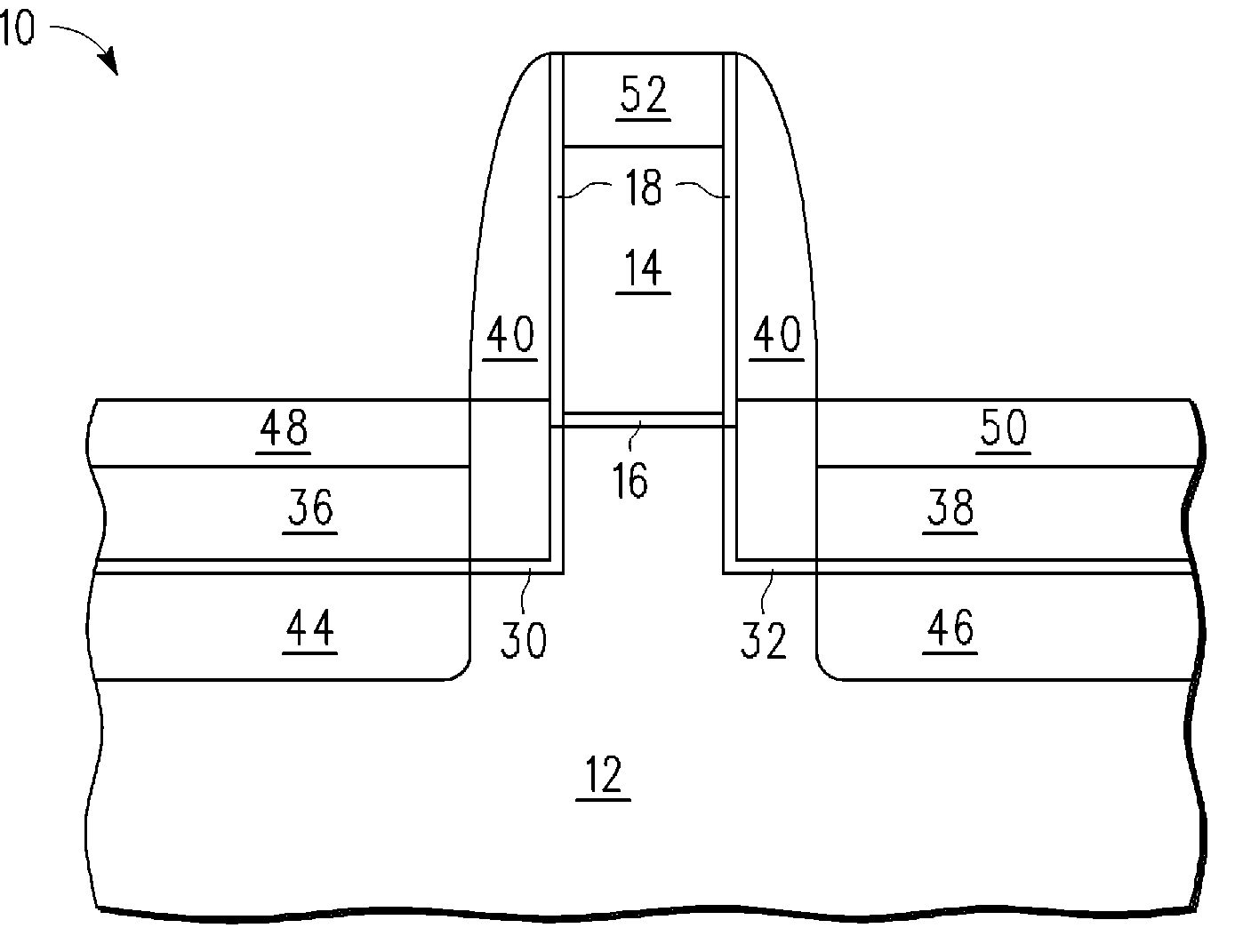
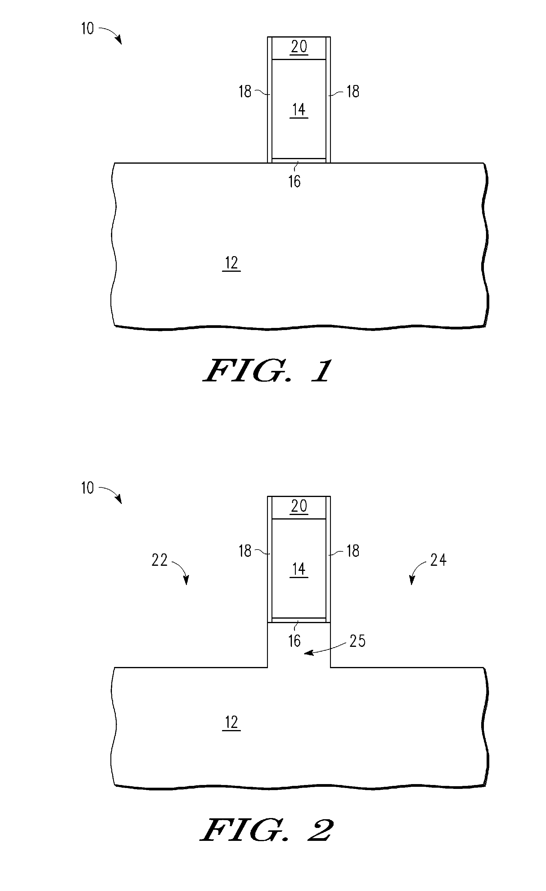
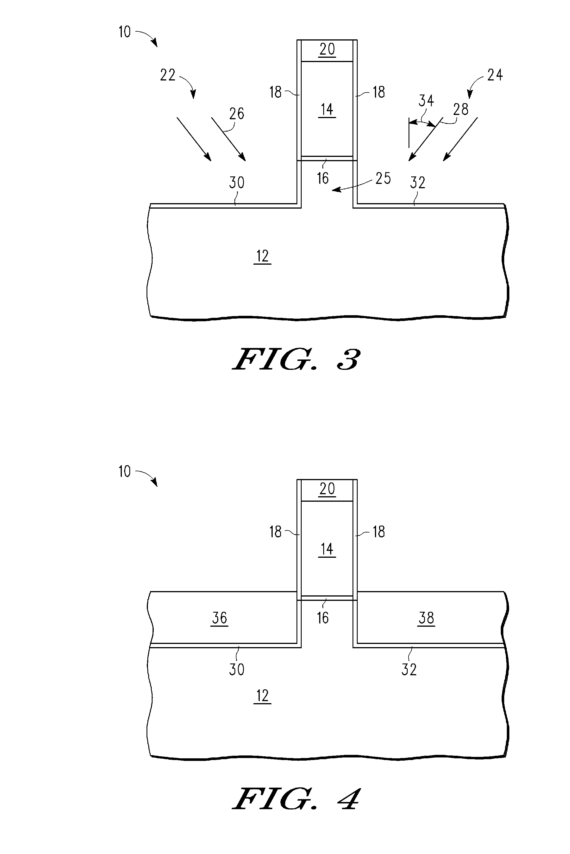
[0014]In one aspect, a semiconductor device is made by forming a gate stack, which is over a semiconductor layer that is used as a mask in recessing the semiconductor layer leaving a semiconductor pillar under the gate stack. Sidewalls of the pillar are doped with nitrogen, or some other dopant blocking species, to form a dopant blocking layer inside the pillar along its sidewall. The recesses are filled with semiconductor material for use as source / drains. There is then a completed transistor having a gate stack over the semiconductor layer that functions as a channel that has at its ends a dopant blocking layer. The dopant blocking layer, which preferably contains nitrogen or carbon for the case where the source / drains have boron as the dopant, which is the typical case for P channel transistors. This is better understood with reference to the drawings and the following description.

[0015]The semiconductor substrate described herein can be any semiconductor material or combinations...


PUM


Abstract

A transistor structure is formed by providing a semiconductor substrate and providing a gate above the semiconductor substrate. The gate is separated from the semiconductor substrate by a gate insulating layer. A source and a drain are provided adjacent the gate to define a transistor channel underlying the gate and separated from the gate by the gate insulating layer. A barrier layer is formed by applying nitrogen or carbon on opposing outer vertical sides of the transistor channel between the transistor channel and each of the source and the drain. In each of the nitrogen and the carbon embodiments, the vertical channel barrier retards diffusion of the source/drain dopant species into the transistor channel. There are methods for forming the transistor structure.

Description

BACKGROUND[0001]1. Field[0002]This disclosure relates generally to semiconductor device structures, and more specifically, to protection of the gate dielectric in transistors.[0003]2. Related Art[0004]Boron penetration into gate dielectrics has been a long standing problem. The boron can come from either the gate side or the channel side. The gate side has generally been the greater problem because of the relatively higher boron concentration. This has been obviated in large measure through techniques using nitrogen or other blocking species such as carbon in the gate or at the top surface of the gate dielectric. Thinner gate dielectrics are desirable for improved transistor performance but are now resulting in an increased susceptibility to boron penetration from the channel side, especially from the source / drains of P channel transistors. Boron penetration has the effect of significantly increasing leakage and subsequently reducing the life of the device. Both gate dielectric leak...

Claims


Application Information

Patent Timeline
IPC IPC(8): H01L21/336H01L29/76
CPCH01L21/26506H01L21/26586H01L29/0847H01L29/7848H01L29/66636H01L29/7834H01L29/165
Inventor ZHANG, DALIU, NINGMOOSA, MOHAMED S.
Owner NORTH STAR INNOVATIONS
Why Eureka
Try Eureka