Vertical channel memory and manufacturing method thereof and operating method using the same

a manufacturing method and technology of vertical channel memory, applied in digital storage, semiconductor devices, instruments, etc., can solve the problems of low memory density, low efficiency, and low efficiency of finfet elements manufactured with high resolution, and achieve the effects of increasing the driving current, improving the memory density, and small dimension

Active Publication Date: 2008-04-17
MACRONIX INT CO LTD
View PDF102 Cites 88 Cited by
  • Summary
  • Abstract
  • Description
  • Claims
  • Application Information

AI Technical Summary

Benefits of technology

[0008]The invention is directed to a vertical channel memory and a manufacturing method thereof and an operating method using the same. A vertical channel transistor structure whose channel width ranges between 10 nm ˜60 nm is manufactured without changing the pitch of the element formed by exposure. The invention effectively increases the driving current during programming or reading without incurring short channel effect or DIBL effect. The FinFET transistor formed thereby has small dimension, hence increasing memory density significantly. Furthermore, the invention provides an SONOS memory with band gap engineered structure, so-called BE-SONOS memory. Compared with the conventional vertical channel memory with SONOS structure, the vertical channel memory with BE-SONOS structure has faster operating speed and wider operating window. The vertical channel memory with BE-SONOS structure can locally trap charge and can enlarge the range of the operating window to achieve an MLC memory.

Problems solved by technology

Despite the photolithography improves continuously, the manufactured planar transistor structure has reached the resolution limit of photolithography, the manufactured transistor element still has the problems of electrostatics discharge (ESD), leakage, reduction in electron mobility, and is apt to short channel effect and drain induced barrier lowering (DIBL) effect.
The manufacturing of FinFET elements with high resolution still requires expensive and advanced manufacturing process by photolithography or E-beam.
However, the throughput of these advance manufacturing processes is difficult to increase and is disadvantageous to large-scale production.
However, the element formed according to such method has poor uniformity and the quality is difficult to control.

Method used


Image

  • Vertical channel memory and manufacturing method thereof and operating method using the same
  • Vertical channel memory and manufacturing method thereof and operating method using the same
  • Vertical channel memory and manufacturing method thereof and operating method using the same

Examples


first embodiment

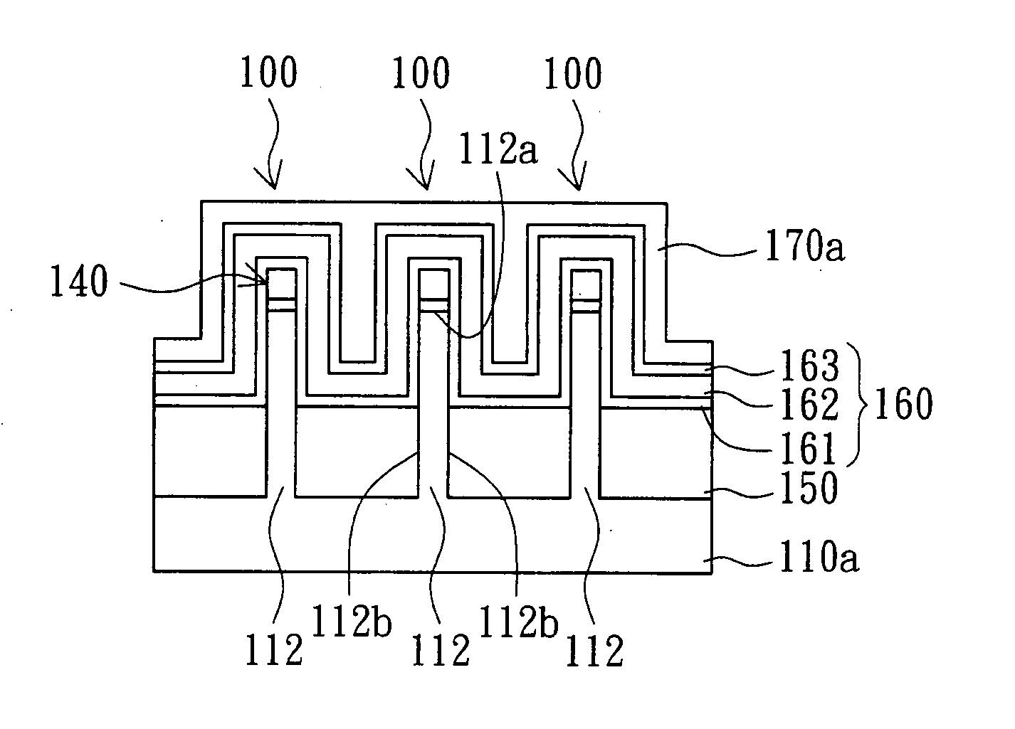
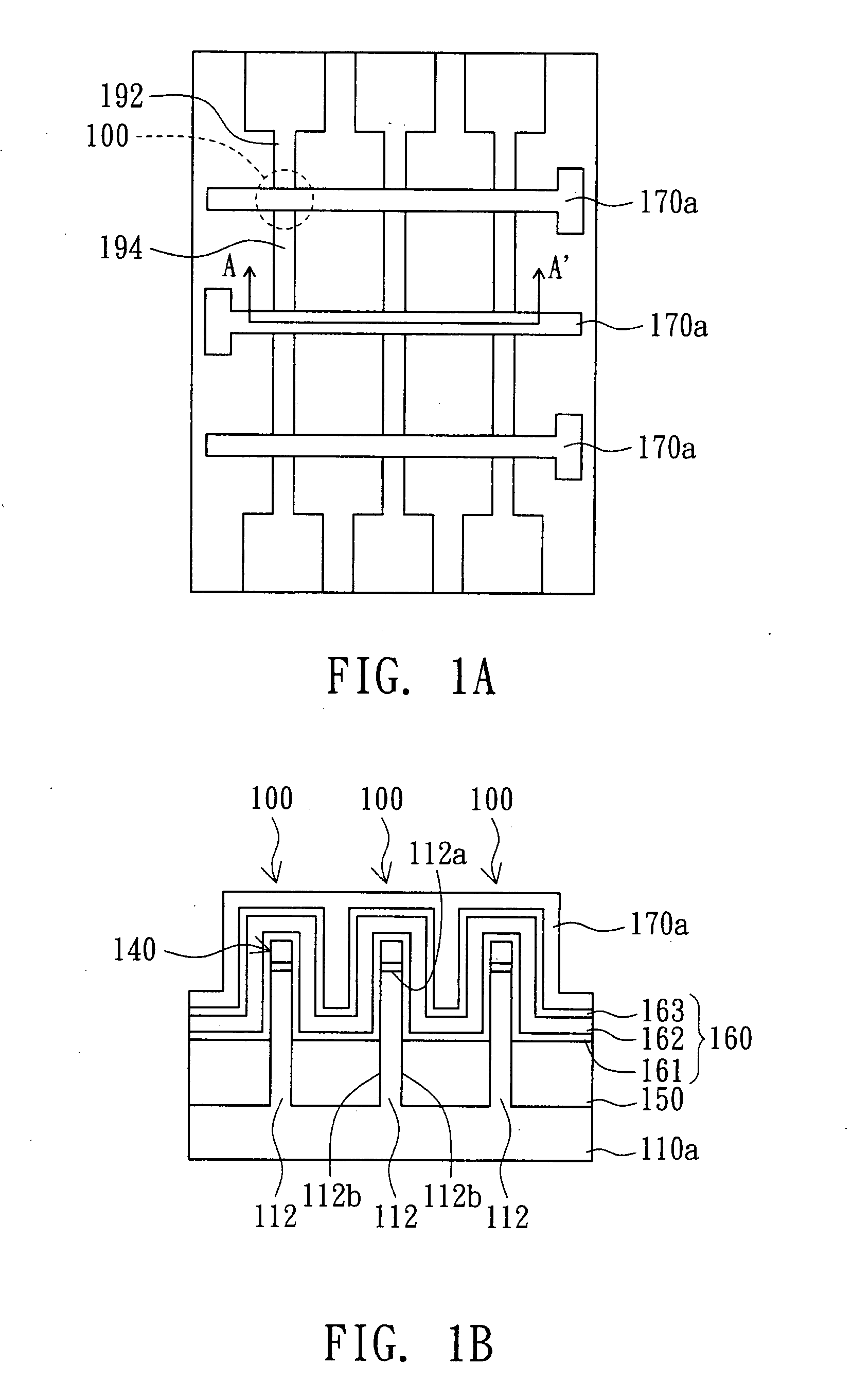
[0025]Referring to FIG. 1A and FIG. 1B. FIG. 1A is a top view of a vertical channel memory according to a first embodiment of the invention. FIG. 1B is a cross-sectional view along a cross-sectional line AA′ of FIG. 1A. As indicated in FIG. 1B, the vertical channel memory 100 includes a substrate 110a, a channel 112 protruded from the substrate 110a and a cap layer 140 disposed on the channel 112. The channel 112 has a top surface 112a and two vertical surfaces 112b. The channel 112 substantially has the same width as that of the cap layer 140. In the present embodiment of the invention, the cap layer 140, an intermediate product during the manufacturing process, includes a silicon dioxide (SiO2) layer and a silicon nitride (SiN) layer, wherein the silicon nitride layer is positioned on the silicon dioxide layer. The cap layer 140 with appropriate thickness avoids the electron penetrating from the gate, therefore avails the formation of a dual channel vertical memory, makes the elec...

second embodiment

[0038]to FIG. 4A and FIG. 4B. FIG. 4A is a top view of a vertical channel memory according to a second embodiment of the invention. FIG. 4B is a cross-sectional view along a cross-sectional line BB′ of FIG. 4A. The vertical channel memory 200 of the present embodiment of the invention differs with the vertical channel memory 100 of the first embodiment in that the cap layer 140 is removed. As for other elements common to the vertical channel memory 100, the same numeric designations are used and the functions are not repeated here.

[0039]As the oxide layer 140 is removed, the top surface of the channel 112 capable of controlling the connection of current by the gate 170a is called a tri-gate structure.

[0040]The application of the present embodiment of the invention is exemplified below by the manufacturing process of the NAND memory array structure. Referring to FIGS. 5A-5J, perspectives illustrating the manufacturing process of the vertical channel memory according to the second emb...

third embodiment

[0051]Referring to FIG. 7A and FIG. 7B, FIG. 7A is a sectional view of a first vertical channel memory according to a third embodiment of the invention. FIG. 7B is a sectional view of a second vertical channel memory according to the third embodiment of the invention. The vertical channel memories 300 and 400 of the present embodiment of the invention differ with the vertical channel memory 100 of the first embodiment and the vertical channel memory 200 of the second embodiment in that the ONO layer 160 is replaced by an multi-layer structure including at least four layers, that is a barrier layer disposed on the channel 112, and a tunneling layer, a charge trapping layer and another barrier layer stacking sequently. In the third embodiment, the multi-layer structure has five layers, that is an ONONO layer 360 having a first barrier layer disposed on the channel 112, and a tunneling layer, a second barrier layer, a charge trapping layer and a third barrier layer stacking sequently, ...


PUM


Abstract

A vertical channel memory including a substrate, a channel, a multi-layer structure, a gate, a first terminal and a second terminal is provided. The channel is protruded from the substrate and has a top surface and two vertical surfaces. The multi-layer structure is disposed on the two vertical surfaces of the channel. The gate straddling multi-layer structure is positioned above the two vertical surfaces of the channel. The first terminal and the second terminal are respectively positioned at two sides of the channel opposing to the gate.

Description

[0001]This is a continuation-in-part application of application Ser. No. 11 / 545,575, filed Oct. 11, 2006.BACKGROUND OF THE INVENTION[0002]1. Field of the Invention[0003]The invention relates in general to a vertical channel memory and a manufacturing method thereof and an operating method using the same, and more particularly to a vertical channel memory with high scalability and a manufacturing method thereof and an operating method using the same.[0004]2. Description of the Related Art[0005]Along with the advance in the manufacturing technology of semiconductor, the resolution of current semiconductor elements has reached nano level. Take the memory for example, the length of the gate and the element pitch are further reduced. Despite the photolithography improves continuously, the manufactured planar transistor structure has reached the resolution limit of photolithography, the manufactured transistor element still has the problems of electrostatics discharge (ESD), leakage, redu...

Claims


Application Information

Patent Timeline
Patent Type & Authority Applications(United States)
IPC IPC(8): H01L29/792G11C11/34H01L21/336
CPCG11C16/0466H01L27/115H01L29/792H01L29/66833H01L29/785H01L27/11568H10B69/00H10B43/30H01L29/513
Inventor HSU, TZU-HSUANLUE, HANG-TING
Owner MACRONIX INT CO LTD
Why Eureka
Try Eureka