Method of forming a transistor having multiple channels

a transistor and channel technology, applied in the field of semiconductor devices, can solve the problems of unfavorable leakage current (i.e. electron or hole flow) between the source and drain, requires significant additional area, and does not offer as much manufacturing control lithographically or spacer defined dimensions

Inactive Publication Date: 2005-07-26
TAIWAN SEMICON MFG CO LTD
View PDF11 Cites 95 Cited by
  • Summary
  • Abstract
  • Description
  • Claims
  • Application Information

AI Technical Summary

Problems solved by technology

Single control of the channel leads to undesired leakage current (i.e. electron or hole flow) between the source and drain when the transistor is intended to be non-conductive.
For example, known planar MOSFETs and FINFETs having multiple channels are formed laterally and thus require significant additional area.
However, lithographically or spacer defined dimensions do not offer as much manufacturing control as grown layers to form a transistor channel.

Method used


Image

  • Method of forming a transistor having multiple channels
  • Method of forming a transistor having multiple channels
  • Method of forming a transistor having multiple channels

Examples


Embodiment Construction

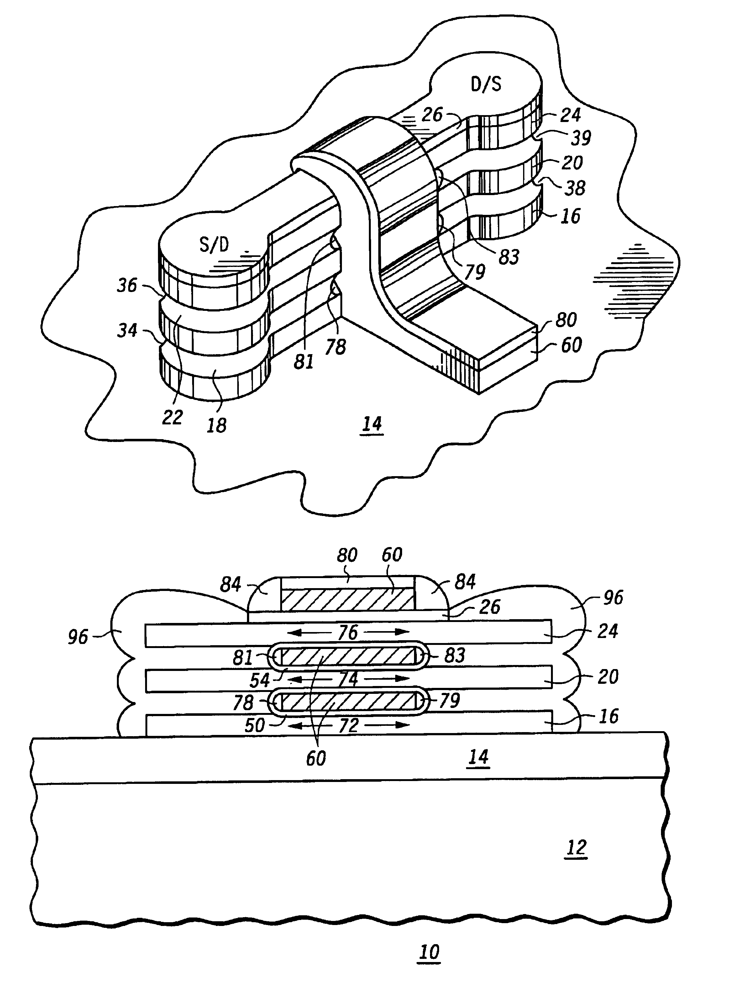
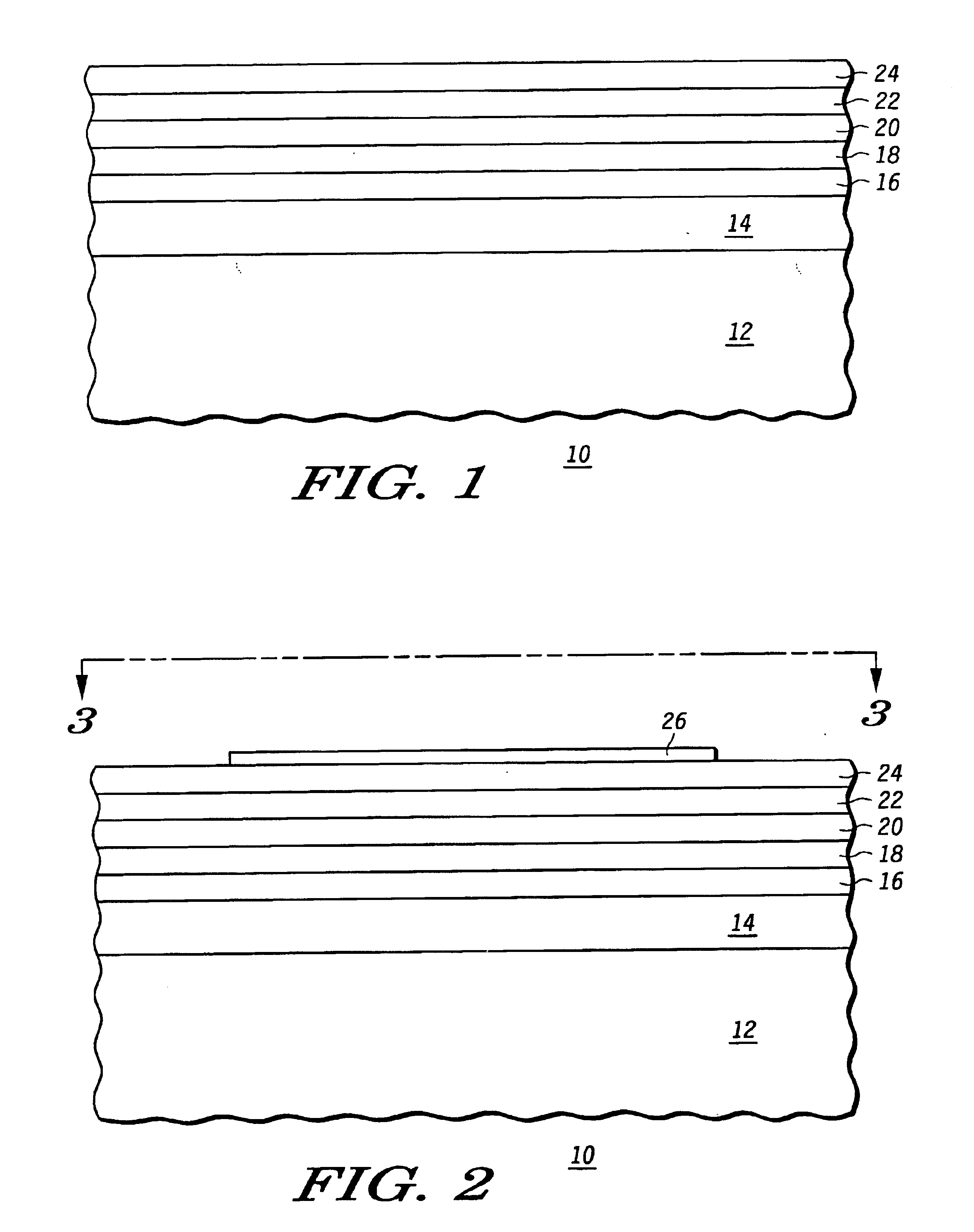
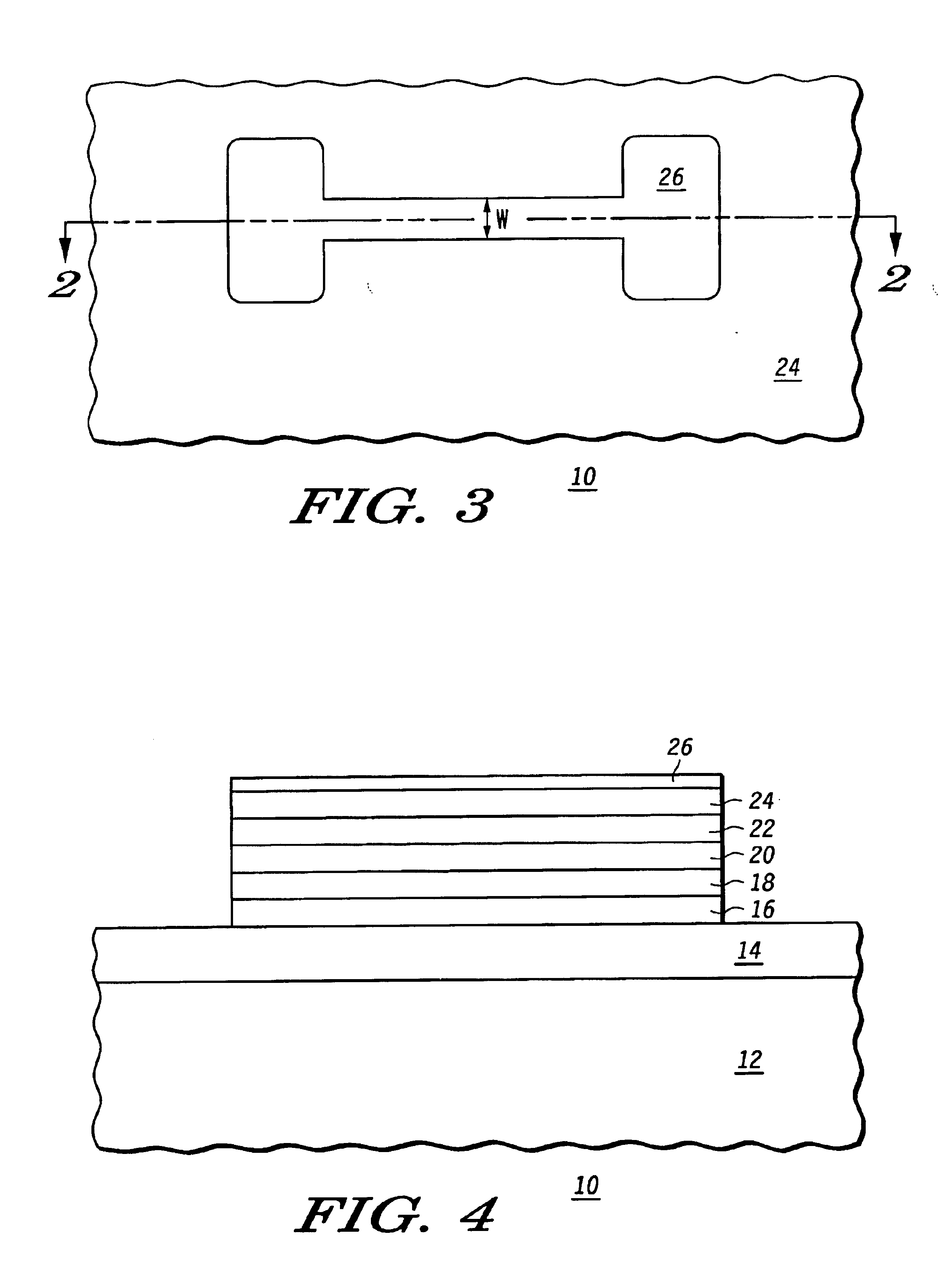
[0019]Illustrated in FIG. 1 is a semiconductor device 10 having a substrate 12. In one form the semiconductor device 10 is an FET (field effect transistor). The substrate 12 may be formed of any type of material, either conductive, semi-conductive or insulative. In one form, substrate 12 is single crystal silicon. Other forms of substrate 12 may include silicon, silicon on insulator, silicon on sapphire, and silicon on nitride. An insulating layer 14 overlies the substrate 12. Insulating layer 14, in one form, is silicon dioxide. Overlying the insulating layer 14 is a semiconductor layer 16. In one form, semiconductor layer 16 is silicon or silicon germanium, but other semiconductor materials may be used. For example, germanium, silicon germanium carbon, gallium arsenide, gallium nitride and indium phosphide are other appropriate material compositions.

[0020]In another form, the integrated circuit substrate 12 is a silicon-on-insulator (SOI) bonded wafer having a silicon layer which ...


PUM


Abstract

A transistor (10) overlies a substrate (12) and has a plurality of overlying channels (72, 74, 76) that are formed in a stacked arrangement. A continuous gate (60) material surrounds each of the channels. Each of the channels is coupled to source and drain electrodes (S / D) to provide increased channel surface area in a same area that a single channel structure is conventionally implemented. A vertical channel dimension between two regions of the gate (60) are controlled by a growth process as opposed to lithographical or spacer formation techniques. The gate is adjacent all sides of the multiple overlying channels. Each channel is formed by growth from a common seed layer and the source and drain electrodes and the channels are formed of a substantially homogenous crystal lattice.

Description

RELATED APPLICATION[0001]This application is related to U.S. patent application Ser. No. 10 / 074,732, entitled “Method of Forming A Vertical Double Gate Semiconductor Device And Structure Thereof” filed Feb. 13, 2002, and assigned to the assignee hereof.FIELD OF THE INVENTION[0002]This invention relates generally to semiconductors, and more specifically, to the manufacture of and the structure of semiconductor devices.BACKGROUND OF THE INVENTION[0003]As semiconductor devices continue to become smaller in size, the devices must be what is known in the industry as “scalable”. That is, the devices must continue to be able to be made with reduced dimensions and still function at the required specifications. Traditionally, MOSFETs have been implemented with a single control electrode or gate on a planar substrate. The gate is placed between a source and drain electrode and functioned to create a channel for controlling the amount of current conducted by the MOSFET. Because there is a gate...

Claims


Application Information

Patent Timeline
Patent Type & Authority Patents(United States)
IPC IPC(8): H01L21/336H01L29/786H01L21/02H01L29/423H01L29/40H01L29/66
CPCH01L29/42384H01L29/66772H01L29/66795H01L29/785H01L29/78654
Inventor ORLOWSKI, MARIUS K.MATHEW, LEO
Owner TAIWAN SEMICON MFG CO LTD
Why Eureka
Try Eureka