Method of forming dual-damascene interconnect structures employing low-k dielectric materials

a dielectric material and interconnecting structure technology, applied in the direction of electrical equipment, semiconductor devices, semiconductor/solid-state device details, etc., can solve the problems of poor metal step coverage along the edges of contact openings, ineffective traditional metal deposition and photolithographic techniques, and difficult control of wet chemical etch processes typically used with metals

Inactive Publication Date: 2003-09-30
NEWPORT FAB
View PDF26 Cites 73 Cited by
  • Summary
  • Abstract
  • Description
  • Claims
  • Application Information

AI Technical Summary

Problems solved by technology

However, the decreasing depth of focus that accompanies this increase in resolution requires the production of highly planar surfaces during intermediary process steps.
In light of the need for highly planar surfaces, traditional metal deposition and photolithographic techniques become progressively more ineffective as line widths are scaled and multiple layers of metal are used.
For example, traditional metal deposition techniques can result in poor metal step coverage along the edges of the contact openings.
Furthermore, wet chemical etch processes typically used with metals are difficult to control.
While dry plasma etching may be employed with many metals, other metals with highly desirable properties (e.g., copper and gold) are generally not amenable to dry etching.
This localized pres

Method used


Image

  • Method of forming dual-damascene interconnect structures employing low-k dielectric materials
  • Method of forming dual-damascene interconnect structures employing low-k dielectric materials
  • Method of forming dual-damascene interconnect structures employing low-k dielectric materials

Examples


Embodiment Construction

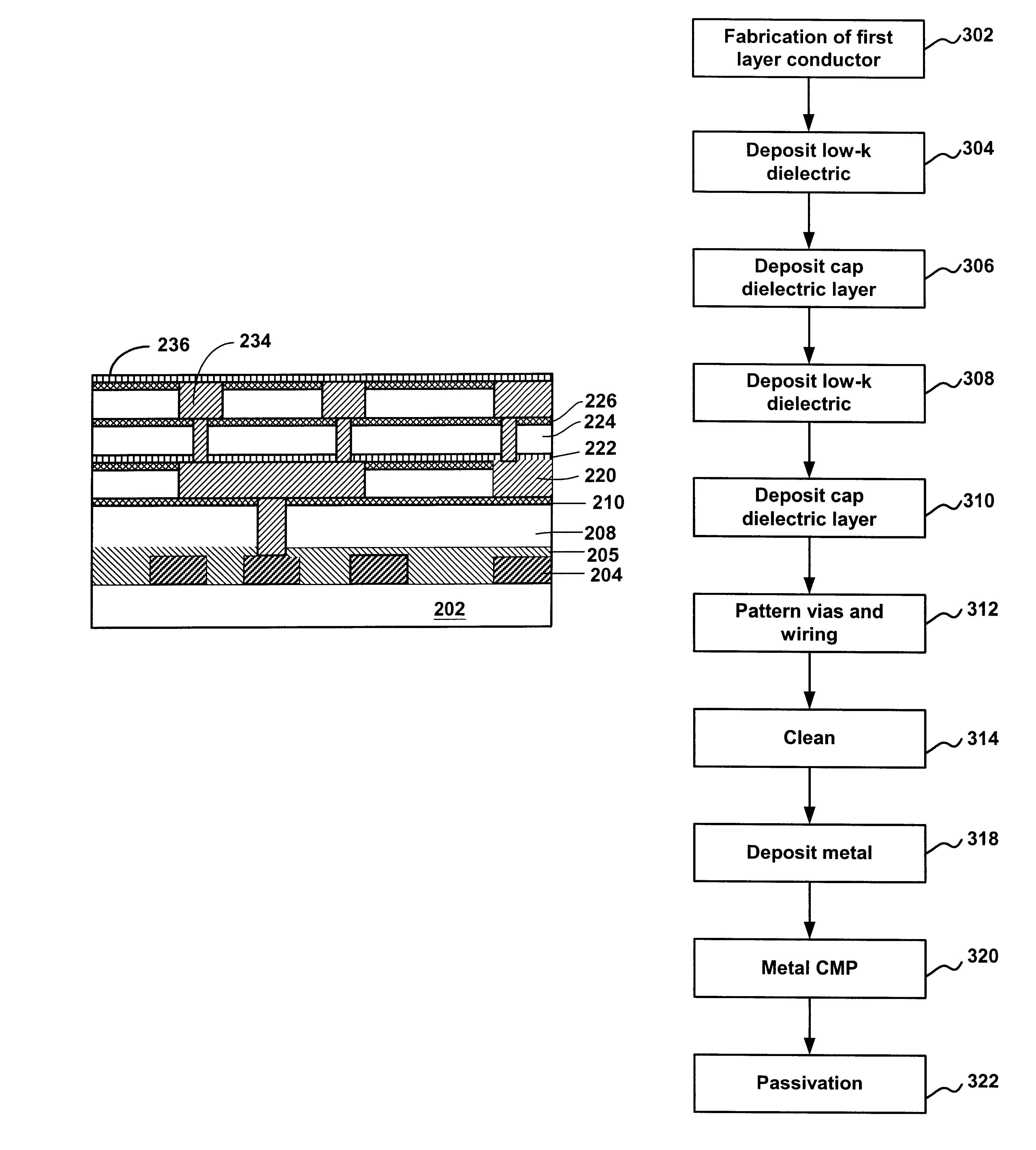
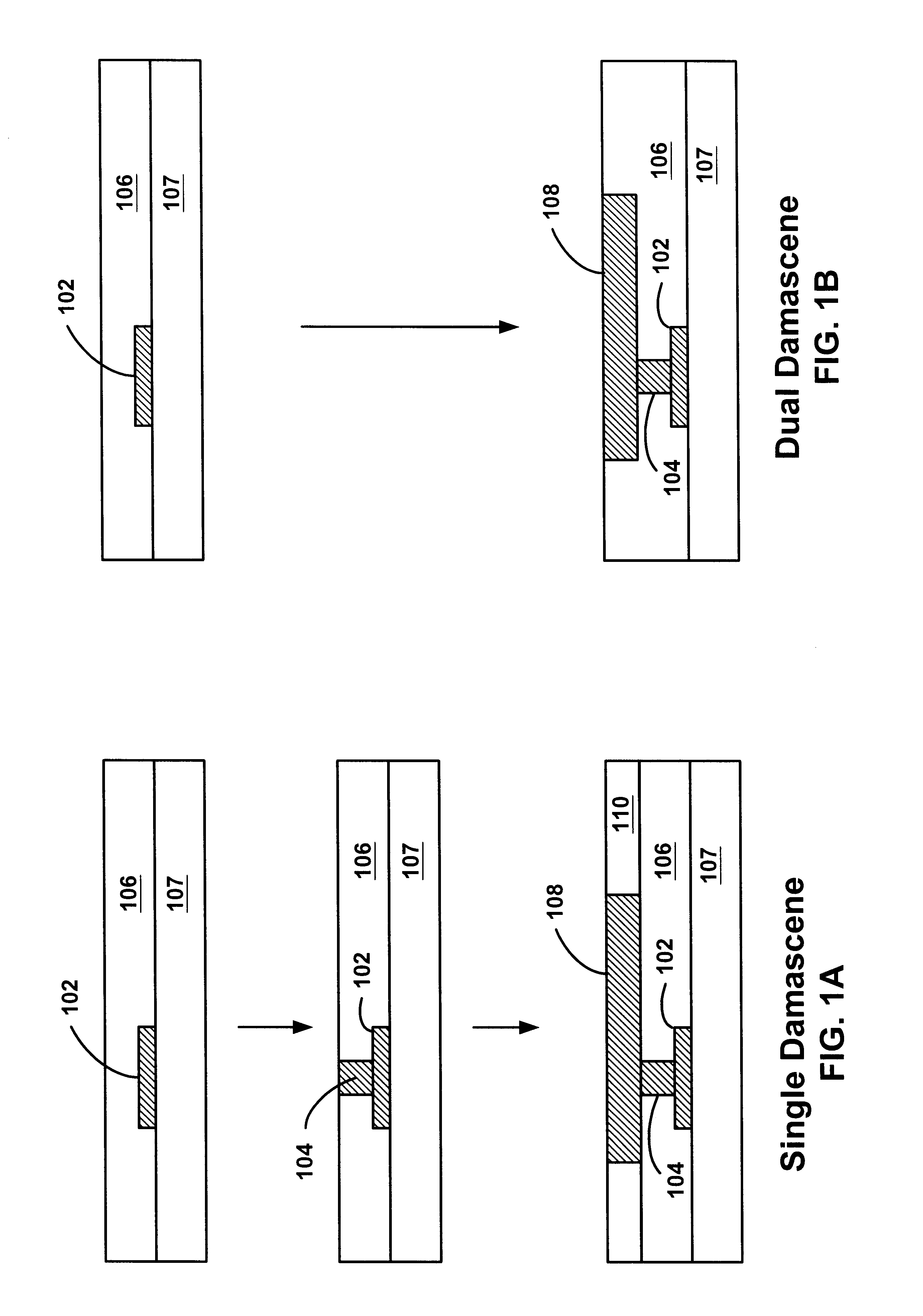
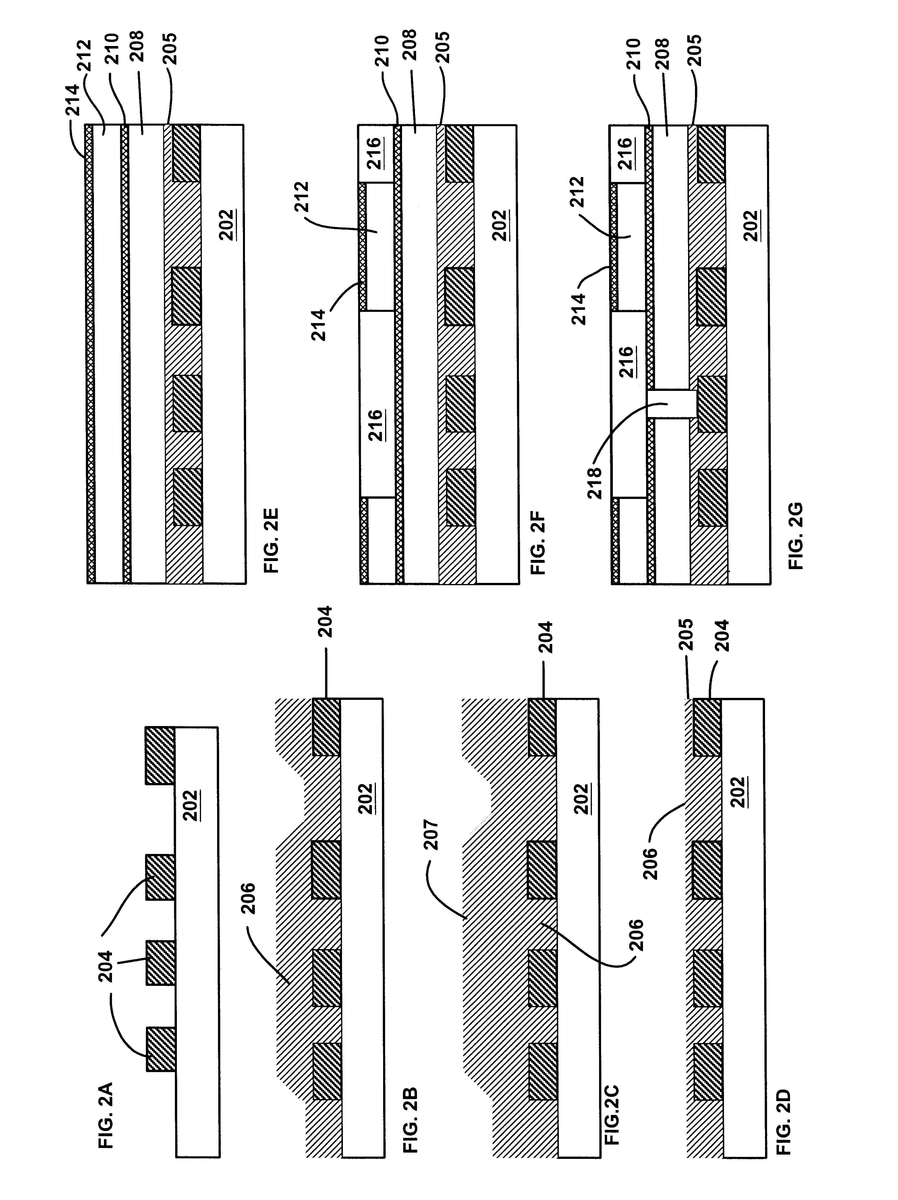
An interconnect fabrication process in accordance with various aspects of the present invention utilizes a dual-damascene scheme incorporating a low-k inter / intra-level dielectric material. With momentary reference to FIG. 2I, a simplified dual-damascene process employs low-k dielectric layers 208 and 212 in conjunction with cap dielectric layers 210 and 214 to form an interconnect metal structure 220 with reduced intralevel and interlevel capacitance. In accordance with an illustrated embodiment, a dual-damascene structure can be implemented without the necessity of using previous single damascene wiring layer, and without CMP of the low-k dielectric.

Referring now to FIGS. 3 and 2A-2L, an interconnect fabrication process in accordance with various aspects of the present invention will now be described in detail. It should be understood that the exemplary process illustrated may include more or less steps or may be performed in the context of a larger processing scheme.

Prior to perf...


PUM


Abstract

Interconnects in sub-micron and sub-half-micron integrated circuit devices are fabricated using a dual damascene process incorporating a low-k dielectric. A dual-damascene structure can be implemented without the necessity of building a single damascene base, and without CMP of the low-k dielectric. This structure simplifies the manufacturing process, reduces cost, and effectively reduces intra-level and inter-level capacitance, resistivity, and noise related to substrate coupling. In accordance with a further aspect of the present invention, a modified silicon oxide material such as silsesquioxane is used for the low-k dielectric in conjunction with silicon dioxide cap layers, allowing an improved process window and simplifying the etching process.

Description

The present invention relates, generally, to methods and structures for multilevel interconnects in integrated circuits using planarization technology and, more particularly, to a dual-damascene approach employing a low-k dielectric.BACKGROUND ART AND TECHNICAL PROBLEMSAdvanced semiconductor processing technology has permitted the fabrication of integrated circuit devices with sub-micron and sub-half-micron features sizes. This trend toward deep submicron technology (i.e., involving feature sizes less than 0.35 microns) has, in turn, driven the need for multilayer interconnects. As a result, circuit performance in the deep submicron regime is increasingly a function of the delay time of electronic signals traveling between the millions of gates and transistors present on the typical integrated circuit chip. Parasitic capacitance and resistance effects resulting from these otherwise passive interconnect structures must therefore be well-controlled. Toward this end, recent trends emph...

Claims


Application Information

Patent Timeline
IPC IPC(8): H01L21/768H01L23/52H01L23/532H01L21/70
CPCH01L21/76807H01L23/5329H01L2924/0002H01L2924/00
Inventor ZHAO, BINBRONGO, MAUREEN R.
Owner NEWPORT FAB
Why Eureka
Try Eureka