Integrated circuit memory devices having error checking and correction circuits therein and methods of operating same

a technology of integrated circuits and memory devices, which is applied in the direction of error detection/correction, error correction/detection using block codes, instruments, etc., can solve the problems of reducing the yield of semiconductor memory devices, and unable to function properly as a whol

Inactive Publication Date: 2004-01-13
SAMSUNG ELECTRONICS CO LTD
View PDF8 Cites 81 Cited by
  • Summary
  • Abstract
  • Description
  • Claims
  • Application Information

AI Technical Summary

Problems solved by technology

Among these memory cells, if even one memory cell does not properly operate, the overall semiconductor memory device cannot function properly.
As the degree of integration of semiconductor memory devices increases, the probability that malfunction occurs in memory cells increases.
Malfunction is caused by defects in the memory cells themselves or by soft errors resulting from the incidence of a particles.
Malfunctioning damages the function of a semiconductor memory device and thus, is a principal cause of reduction i

Method used


Image

  • Integrated circuit memory devices having error checking and correction circuits therein and methods of operating same
  • Integrated circuit memory devices having error checking and correction circuits therein and methods of operating same
  • Integrated circuit memory devices having error checking and correction circuits therein and methods of operating same

Examples


Embodiment Construction

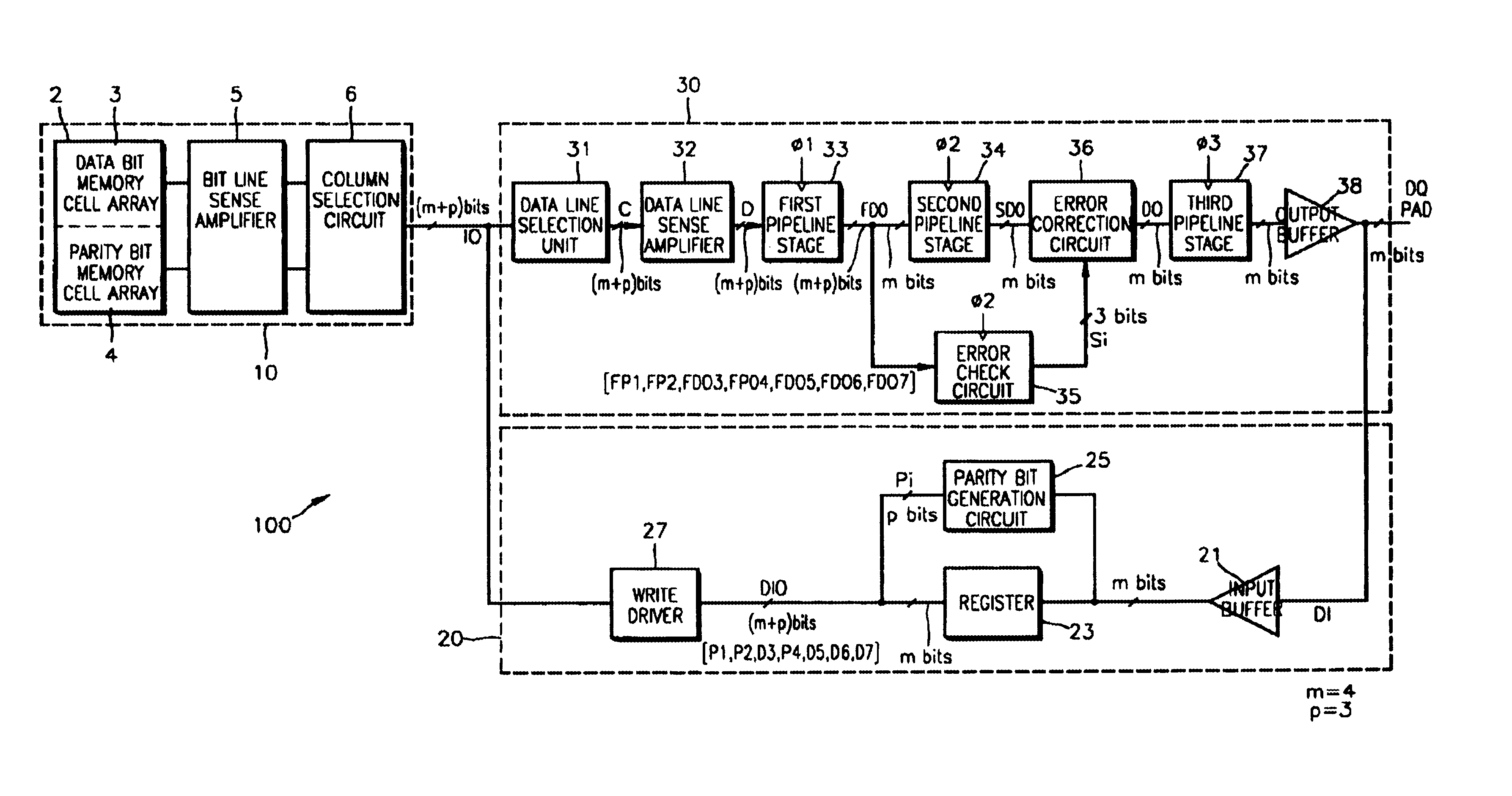
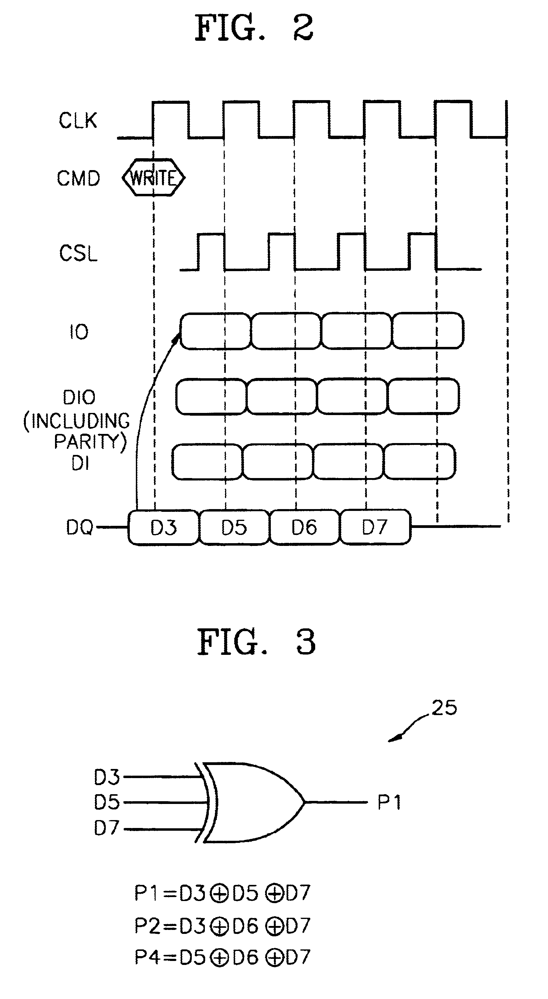
The present invention will now be described more fully with reference to the accompanying drawings, in which preferred embodiments of the invention are shown. The same reference numerals in different drawings represent the same element. The description of the present invention concerns a synchronous DRAM (SDRAM) having a pipeline data structure, in which the SDRAM operates in synchronization with a clock signal and previously generates internal data to support the high speed of data which is input from or output to the outside. The composition of input / output data bits of different SDRAMs varies, but this specification describes a case in which input / output data bits are composed of m (=4) bits and parity bits are composed of p (=3) bits corresponding to the m (=4) bits.

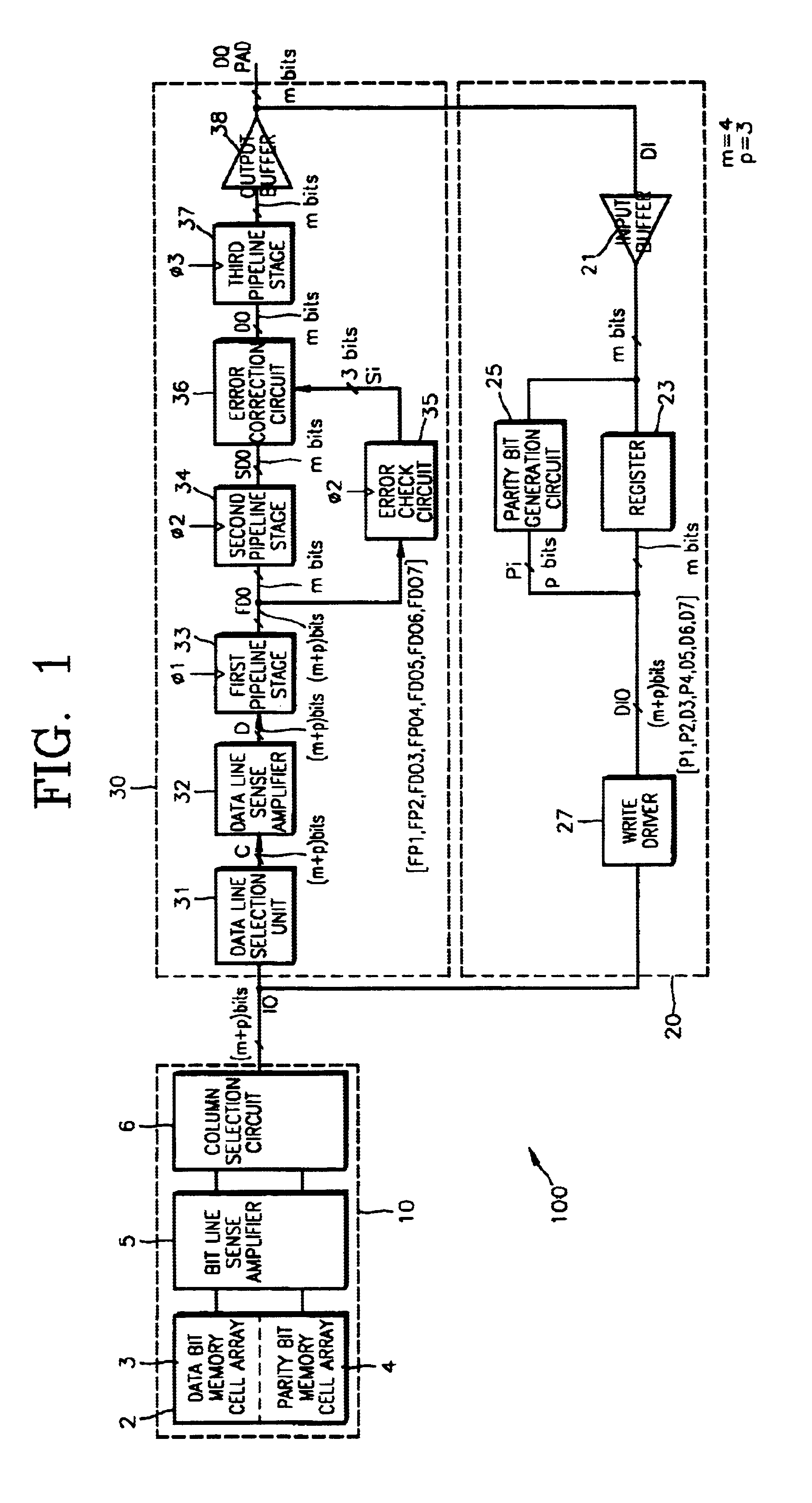
FIG. 1 is a diagram of a synchronous semiconductor memory device having a error check and correction (ECC) circuit according to an embodiment of the present invention. Referring to FIG. 1, a synchronous semiconductor...


PUM


Abstract

Integrated circuit memory devices include a memory cell array having therein a plurality of stored data bits and a plurality of parity bits generated from a plurality of write data bits received by the memory device during a write operation. The plurality of stored data bits and the plurality of parity bits may collectively form a word having a length of m+p bits, where m and p are integers. An error check circuit is provided that converts the plurality of stored data bits and the plurality of parity bits into a plurality of syndrome bits (e.g., Si) that designate a location of a bit error in the plurality of stored data bits when compared against the original write data bits. An error correction circuit is provided that uses the plurality of syndrome bits to correct an error in the plurality of stored data bits and generate a plurality of read data bits that match the plurality of original write data bits.

Description

This application is related to Korean Application No. 99-32908, filed Aug. 11, 1999, the disclosure of which is hereby incorporated herein by reference.FILED OF THE INVENTIONThe present invention relates to semiconductor memory devices, and more particularly, to semiconductor memory devices having on-chip error correction capability.BACKGOUND OF THE INVENTIONDue to the recent development of micro technology, semiconductor devices can be designed to be highly integrated and operate at high speed. Particularly for high integrated semiconductor memory devices, a high yield is desired.A semiconductor memory device is composed of many memory cells. Among these memory cells, if even one memory cell does not properly operate, the overall semiconductor memory device cannot function properly. As the degree of integration of semiconductor memory devices increases, the probability that malfunction occurs in memory cells increases. Malfunction is caused by defects in the memory cells themselves...

Claims


Application Information

Patent Timeline
IPC IPC(8): G06F12/16G11C29/00G11C29/42
CPCG06F11/1024H03M13/13G11C2029/0411G11C29/00
Inventor LEE, JUNG-BAE
Owner SAMSUNG ELECTRONICS CO LTD
Why Eureka
Try Eureka