LSI having a built-in self-test circuit

a self-testing, silicon-based technology, applied in the direction of instruments, pulse automatic control, solid-state devices, etc., can solve the problem of high cost of speed ic testers

Inactive Publication Date: 2004-02-03
NEC ELECTRONICS CORP
View PDF20 Cites 17 Cited by
  • Summary
  • Abstract
  • Description
  • Claims
  • Application Information

AI Technical Summary

Problems solved by technology

However, since the higher-speed IC tester is expensive, it is desired to test the higher-speed LSI by using on ordinary IC tester operating at a lower speed and thus being less expensive.

Method used


Image

  • LSI having a built-in self-test circuit
  • LSI having a built-in self-test circuit
  • LSI having a built-in self-test circuit

Examples


first embodiment

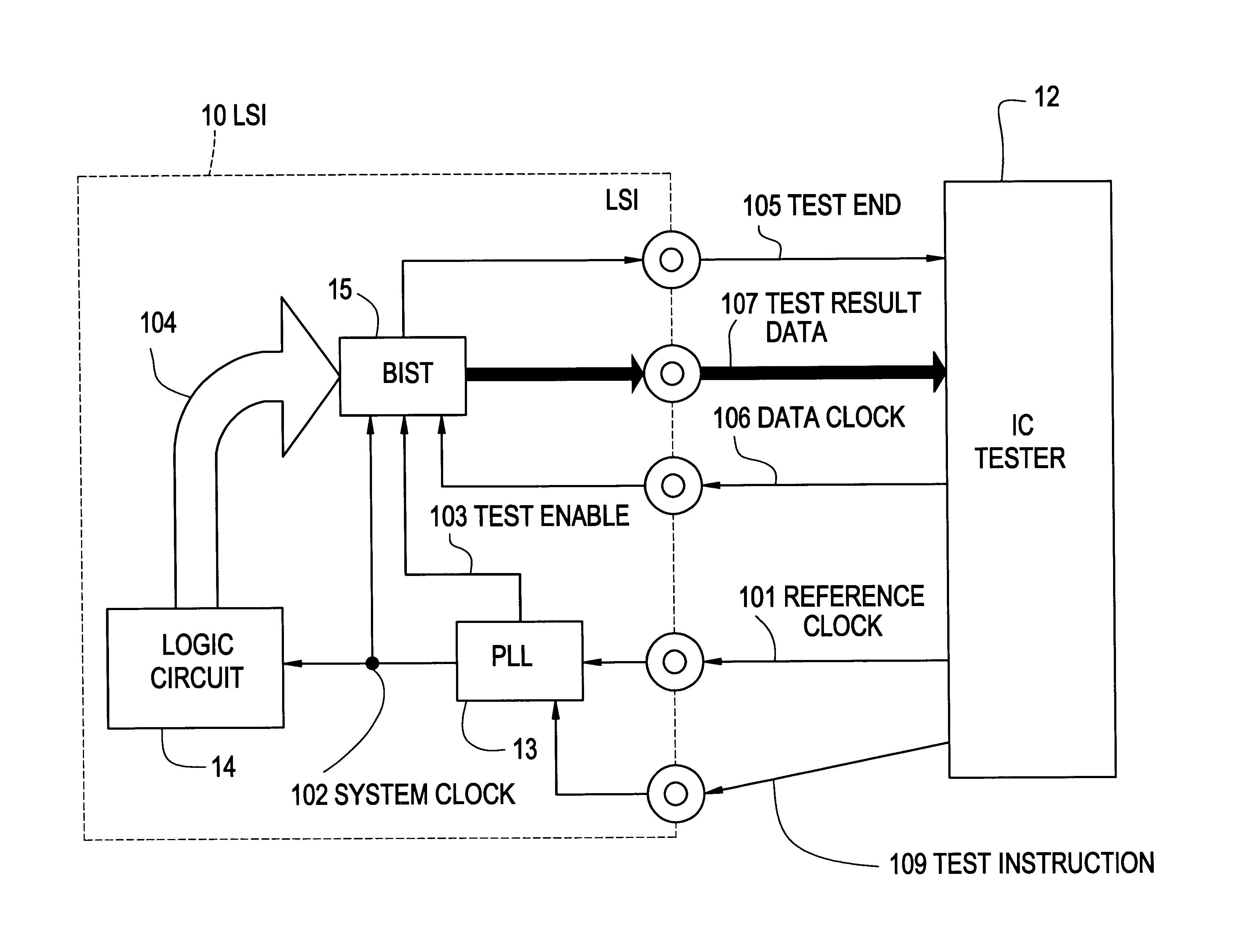
Referring to FIG. 3, a LSI, generally designated by numeral 10, according to the present invention includes a logic circuit 14, a PLL circuit 13 and a BIST circuit, and is subjected to a functional self-test based on the instruction from the IC tester 12.

The PLL circuit 13 receives a reference clock signal 101 from the IC tester 12, generates an internal system clock signal 101 therein by multiplication of the frequency of the reference clock signal 101, and compares the phase of the system clock signal 102 against the phase of the reference clock signal 101 to generate a phase lock signal after the coincidence of the phase therebetween. The system clock signal 102 is delivered to the logic circuit 14 and the BIST circuit 15.

The logic circuit 14 has a design function, operates with the system clock signal 102 for signal processing, and delivers output signal therefrom during a normal operation as well as a functional test operation thereof.

The BIST circuit 15 includes a test pattern...

second embodiment

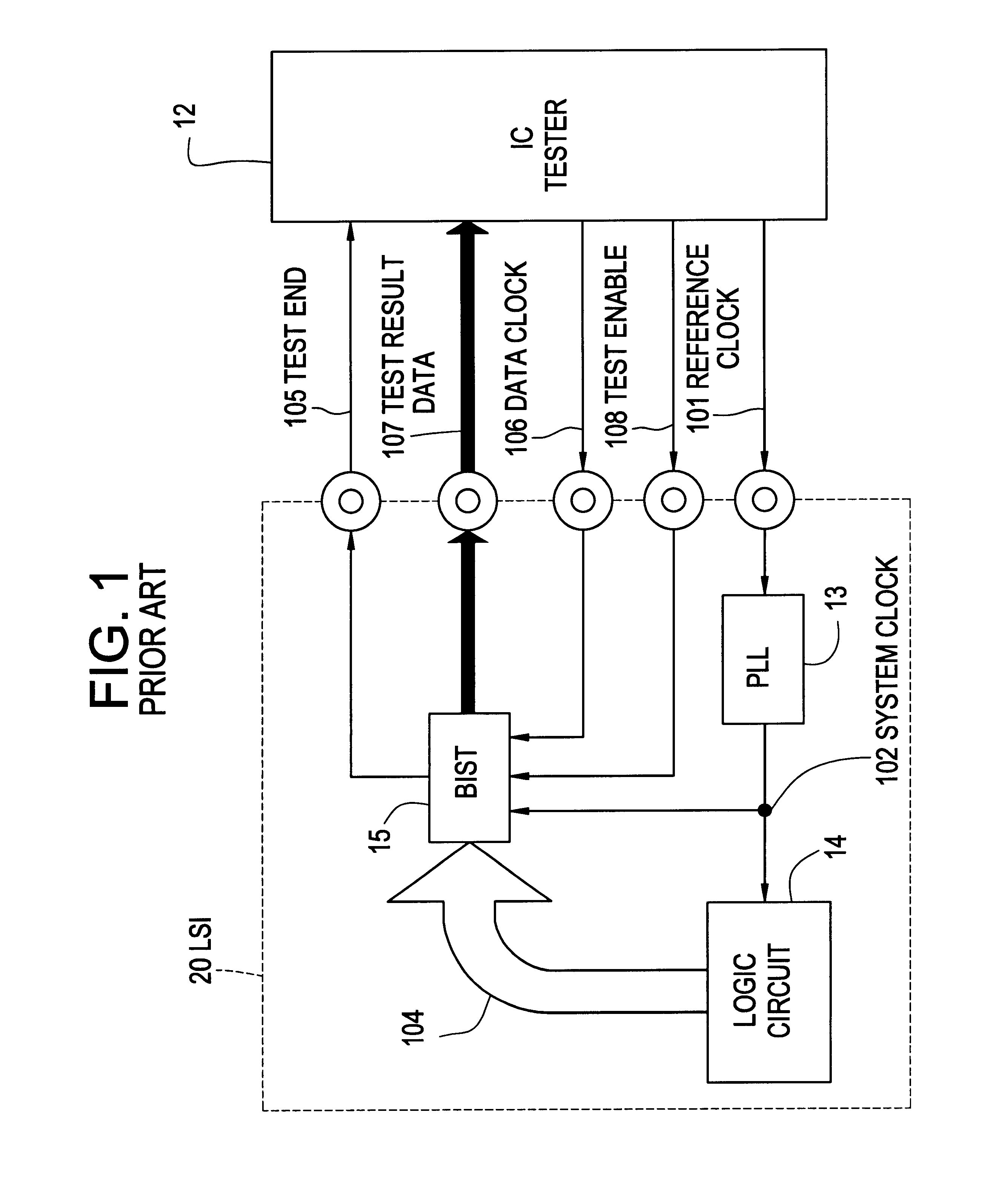
Referring to FIG. 5, an IC test for a LSI according to the present invention is different from the IC test shown in FIG. 3 in that the LSI 10A transmits the test result data 107 and the data clock signal 106 to the IC tester 12 without transmitting the test end signal after the self-test is finished by the BIST circuit 15.

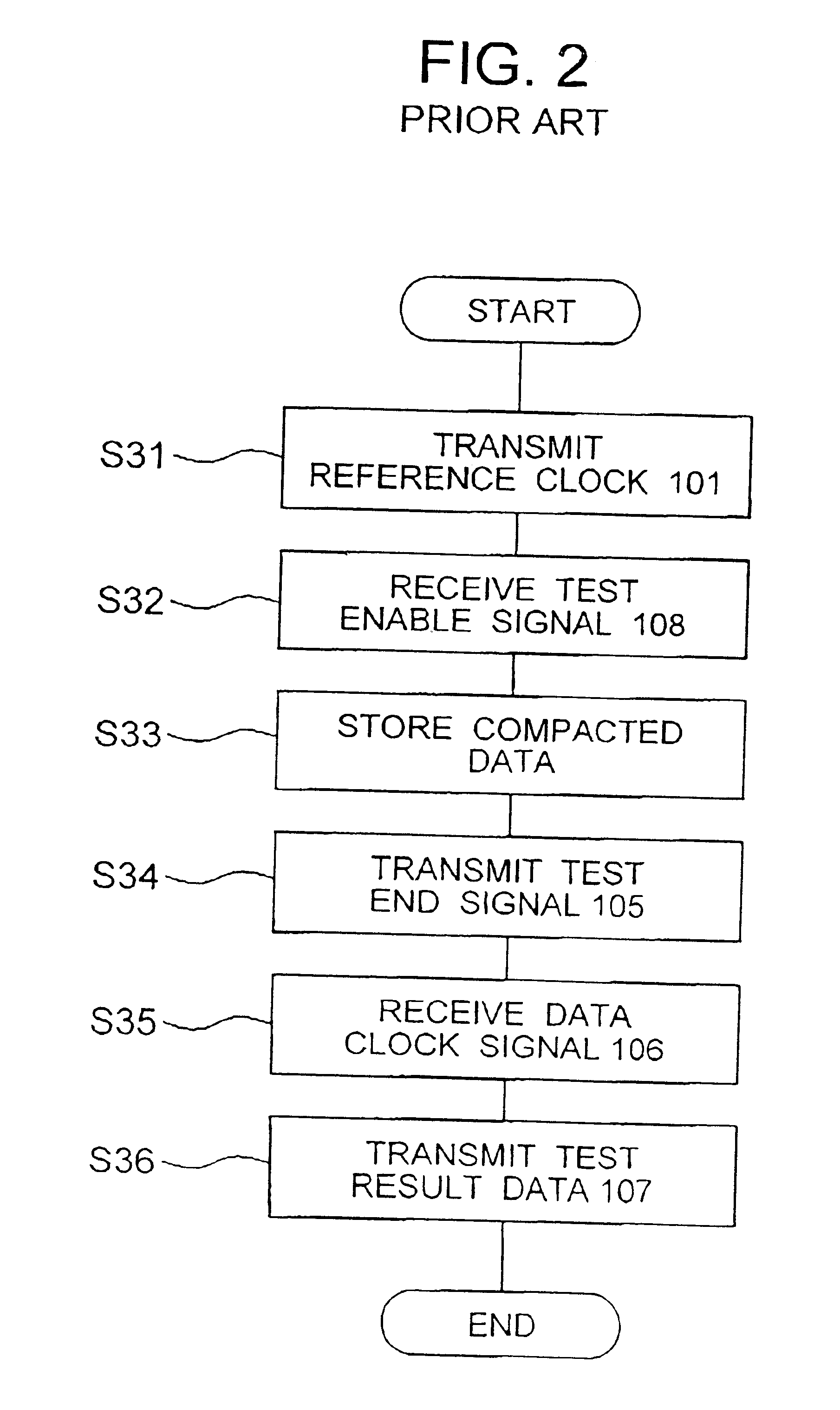
Referring to FIG. 6, steps S21 to S24 in the second embodiment are similar to steps of S11 to S14, respectively, in the first embodiment. In the present embodiment, the BIST circuit 15 transmits the data clock signal 106 and the test result signal 107 to the IC tester 12 in step S25 by a serial data transmission.

In the present embodiment, since the IC tester need not transmit the data clock signal 106, the circuit structure of the IC tester 12 can be simplified and the time length for the self-test can be also reduced.


PUM


Abstract

A LSI includes a logic circuit, a PLL circuit and a built-in self-test (BIST) circuit. When the PLL circuit detects a phase lock of the system clock signal of the LSI with a reference clock signal under the condition of presence of a test instruction signal, the PLL delivers a test enable signal to the BIST circuit. The BIST circuit responds to the test enable signal to test the logic circuit in a functional test. The BIST circuit transmits the test result data to an IC tester after the functional test. Throughput of the functional test can be improved by eliminating transmission of the test enable signal from the IC tester to the LSI.

Description

(a) Field of the InventionThe present invention relates to a semiconductor large-scale integrated circuit (LSI) having a built-in self-test (BIST) circuit and, more particularly, to improvement of a BIST circuit installed in a LSI for testing the function of the logic circuit in the LSI.(b) Description of the Related ArtIC tester is generally used In a test operation of a LSI. In a test operation of a high-speed LSI, the IC tester operates in a series of processing for the LSI, including transmitting a test pattern for operating the LSI, receiving resultant data from the LSI, comparing the resultant data against the expected data and judging pass / fail of the LSI. The series of the processing should be performed in accordance with the operational speed of the LSI under test, and thus the higher-speed LSI should be tested by the IC tester operating at a higher speed. However, since the higher-speed IC tester is expensive, it is desired to test the higher-speed LSI by using on ordinary...

Claims


Application Information

Patent Timeline
Patent Type & Authority Patents(United States)
IPC IPC(8): G01R31/28G01R31/3183H01L21/822H01L27/04H03L7/08
CPCG01R31/2884
Inventor FUKUDA, YASUHIRO
Owner NEC ELECTRONICS CORP
Why Eureka
Try Eureka