Semiconductor integrated circuit, design support apparatus, and test method

a technology of integrated circuits and support devices, applied in memory systems, program control, instruments, etc., can solve problems such as inability to obtain information necessary for analyzing failures, failures that are sometimes analyzed, and lengthen the design time required until scan becomes possibl

Inactive Publication Date: 2003-12-11
KK TOSHIBA
View PDF2 Cites 48 Cited by
  • Summary
  • Abstract
  • Description
  • Claims
  • Application Information

AI Technical Summary

Problems solved by technology

As a result, for an LSI having the failure, the failure is sometimes analyzed.
In this case, as described above, since the information indicating the presence / absence of the failure is compressed inside the LSI in the test using the logic BIST circuit, the information necessary for analyzing the failure cannot be obtained as such.
However, when the logic BIST circuit is used to analyze the failure as described above, there are several problems as follows.
Moreover, it is necessary to separately prepare the scan test pattern, and as a problem, a design time required until the scan becomes possible lengthens.
Therefore, the failure which can be detected only by a logic BIST operation cannot be analyzed.
This is an important problem, when an actual operation rate test is carried out by the logic BIST operation.

Method used


Image

  • Semiconductor integrated circuit, design support apparatus, and test method
  • Semiconductor integrated circuit, design support apparatus, and test method
  • Semiconductor integrated circuit, design support apparatus, and test method

Examples


second embodiment

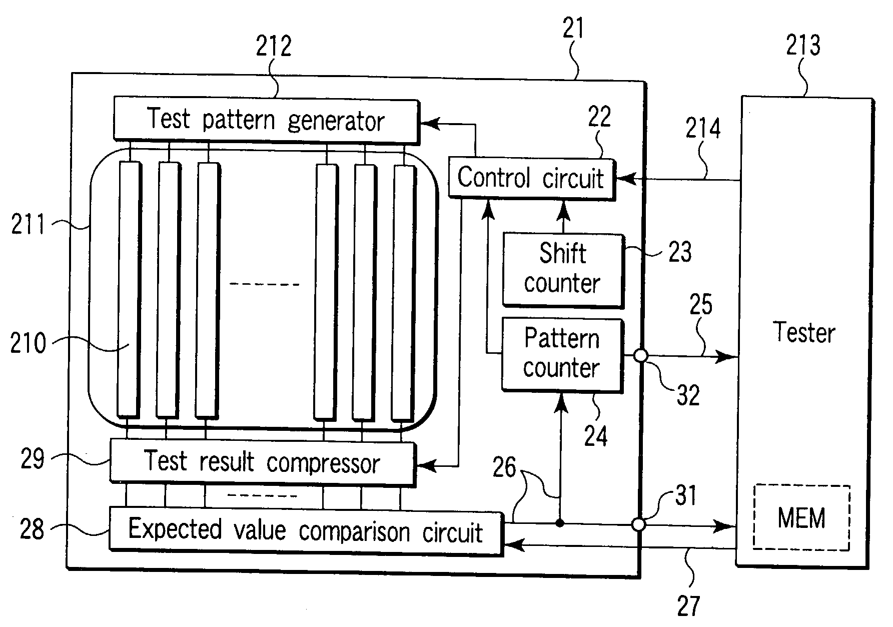
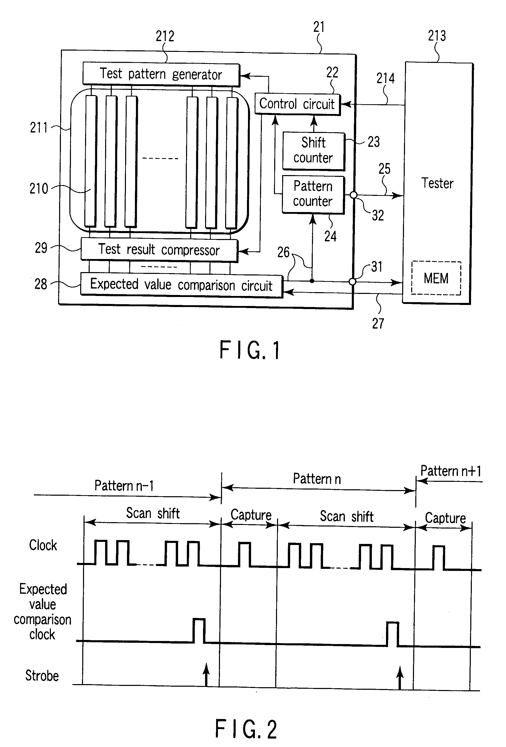
[0134] In the same manner as in the second embodiment, the expected value comparison circuit 1011 compares the output signal of each selector 1107 with the expected value signal 1010 which is the expected value supplied from the tester 1016 for each bit shift. When this result is mismatch, the expected value comparison circuit 1011 outputs the failure flag 1009. The shift counter 1003 outputs the failure shift count signal 1004 in response to the failure flag 1009 supplied via the gate 1007. The tester 1016 records the bit string of the failure flag 1009 and the failure shift count signal 1004 in a failure log 1807.

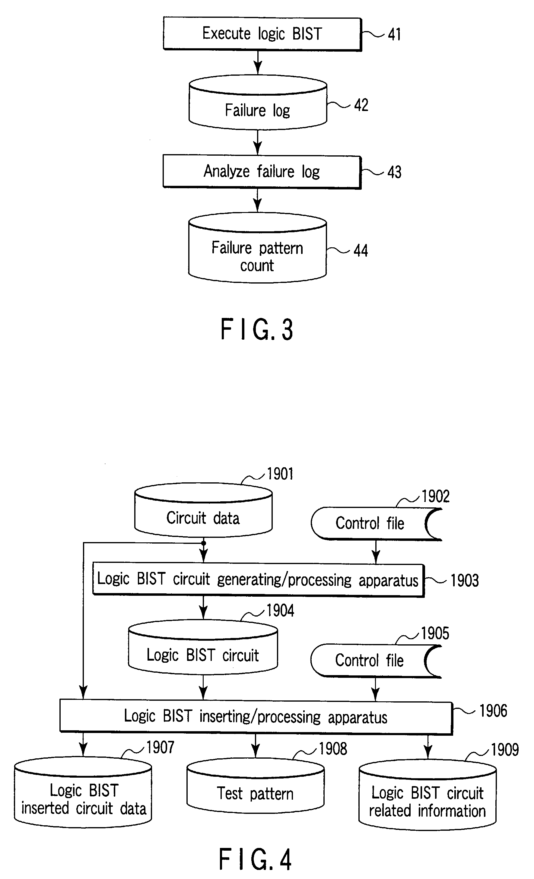
[0135] As a result of the second logic BIST, the information of the failure scan chain and failure shift count is stored in the failure log 1807. In the analysis of the second failure log (step 1808), information 1809 of the failure scan chain and failure shift count is extracted. Moreover, since the failure shift count is already obtained in the first failure log analysi...

third embodiment

[0136] As described above, according to the logic BIST circuit the selector circuit is used to reduce the number of output signals of the test result compressor 1012. Therefore, even when the number of internal scan chains is larger than the number of pins for scan input / output of the tester 1016, the failure can be analyzed. Therefore, restriction required in the design of the logic BIST can be relaxed.

[0137] The design support apparatus described in the first embodiment and shown in FIG. 4 can also be applied to the design of the logic BIST circuit shown in FIG. 9. Moreover, in the same manner as in the second embodiment, the information of the failure scan flip-flop corresponding to the failure shift and failure scan chain is included in output data 1909 concerning the logic BIST output from the design support apparatus of FIG. 4, and thereby the failure scan flip-flop can be specified only by referring to the data.

[0138]

[0139] Additionally, when a plurality of XOR gates 1108 a...

fourth embodiment

[0147] FIG. 15 shows a whole constitution of the design support apparatus which constitutes the logic BIST circuit including the scan chain shown in FIG. 14.

[0148] This design support apparatus is roughly constituted of a scan flip-flop dependence relationship extracting / processing apparatus 1402 and scan chain constructing / processing apparatus 1404.

[0149] The scan flip-flop dependence relationship extracting / processing apparatus 1402 reads a net list 1401, lists up the scan flip-flops influenced by the signal line from the net list, and outputs scan flip-flop dependence information 1403. The scan chain constructing / processing apparatus 1404 reads the scan flip-flops dependence information 1403 and net list 1401, and constructs the scan chain in which the data simultaneously influenced by the failure is not supplied to the XOR gate.

[0150] In this processing, either before or after the scan chain is extended, arrangement wiring information is also used to construct the scan chain, a...


PUM


Abstract

There is disclosed a semiconductor integrated circuit comprising a logic BIST circuit which includes a test pattern generator and test result compressor and which performs a built-in self test (logic BIST) of a logic circuit, a pattern counter which counts test patterns during the logic BIST, an expected value comparison circuit which compares a compressed value output of the test result compressor with an expected value input from an external tester for each test pattern and which outputs a failure flag at a mismatch detection time, an external terminal which outputs the failure flag from the LSI, and an external terminal which outputs from the LSI a pattern count signal at a time when the pattern counter receives the failure flag.

Description

[0001] This application is based upon and claims the benefit of priority from the prior Japanese Patent Application No. 2002-133186, filed May 8, 2002, the entire contents of which are incorporated herein by reference.[0002] 1. Field of the Invention[0003] The present invention relates to a semiconductor integrated circuit (LSI), design support apparatus, and test method, particularly to a logic built-in self-test (BIST) circuit, design support apparatus, and test method, and is applied to, for example, a logic system LSI.[0004] 2. Description of the Related Art[0005] As one of the test facilitating methods for solving the difficulty of testing a large and complicated LSI, a logic BIST is used. In the logic BIST, the generation of the test pattern given to a block to be tested, and analysis of the test result output from the block to be tested, are all automatically performed in the LSI by a logic circuit constituted in the periphery of the block to be tested.[0006] FIG. 16 shows a ...

Claims


Application Information

Patent Timeline
Patent Type & Authority Applications(United States)
IPC IPC(8): G01R31/3183G01R31/28G01R31/3185G06F9/44G06F17/50H01L21/822H01L27/04
CPCG01R31/318563G01R31/318569G01R31/318566
Inventor HASEGAWA, TETSUANZOU, KENICHI
Owner KK TOSHIBA
Why Eureka
Try Eureka