
Method and apparatus for programmable logic device (PLD) built-in-self-test (BIST)

Inactive Publication Date: 2005-01-04
CYPRESS SEMICON CORP
View PDF23 Cites 60 Cited by
  • Summary
  • Abstract
  • Description
  • Claims
  • Application Information

AI Technical Summary

Problems solved by technology

Such an approach can be time consuming as a tester must apply various input signals and wait for the resulting input signals.
A drawback to conventional programmable logic BIST has been the resulting area that BIST circuits require.
Such additional area can increase the overall size the resulting devices, increasing manufacturing costs.
In addition to increasing overall area, the incorporation of such “hard” logic circuits into the existing logic circuits can add complexity to the design, complicating circuit layout and routing.
Added complexity arises out of the need to include such hard logic BIST circuits without adversely affecting normal mode signal propagation times.
While a conventional assembly 800 such as that shown in FIGS. 8A to 8C can provide BIST functionality, it comes at the cost of increased circuit area on a PLD 804.

Method used


Image

  • Method and apparatus for programmable logic device (PLD) built-in-self-test (BIST)
  • Method and apparatus for programmable logic device (PLD) built-in-self-test (BIST)
  • Method and apparatus for programmable logic device (PLD) built-in-self-test (BIST)

Examples


fourth embodiment

As noted above, alternate embodiments could include more than one self-test. FIGS. 7A-7D illustrate a fourth embodiment that can include multiple tests and multiple nonvolatile memory sectors having different properties.

A fourth embodiment 700 may include a nonvolatile memory 702, a volatile PLD 704, and a test port 706. A nonvolatile memory 702 may include multiple sectors. two of which are shown as 708-0 and 708-1. Sectors (708-0 and 708-1) may have different properties. In particular, such sectors may be separately erasable and one may be a “boot” sector. Boot sectors are well understood in the art any may include various protection features that prevent boot data from being erased and / or overwritten.

In the example of FIGS. 7A to 7D it will be assumed that sector 708-0 may be a boot sector that includes BIST data for a particular test BIST0. Sector 708-1 may be a non-boot sector that includes BIST data for a second test BIST1. Such an arrangement may be advantageous when the freq...


PUM


Abstract

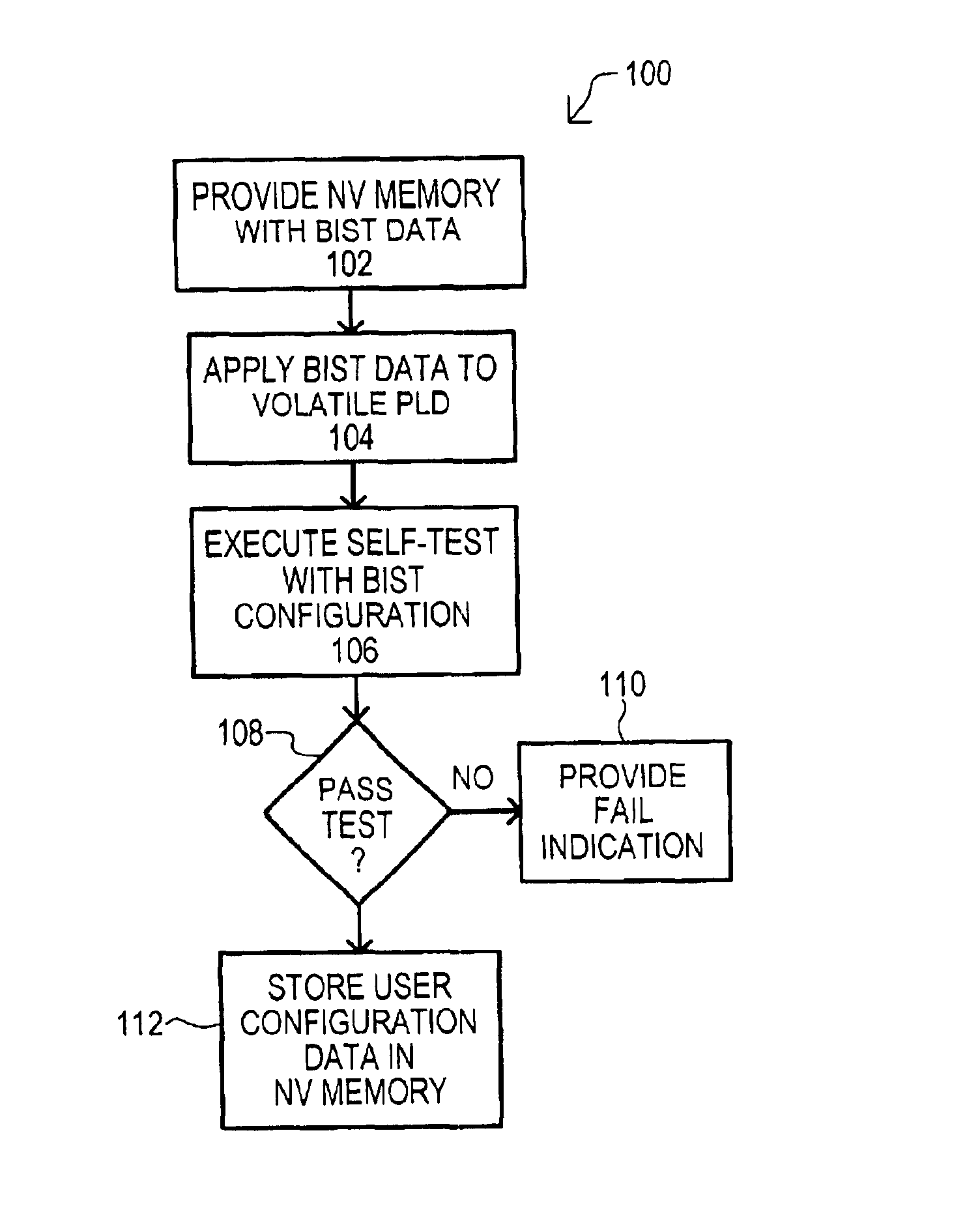
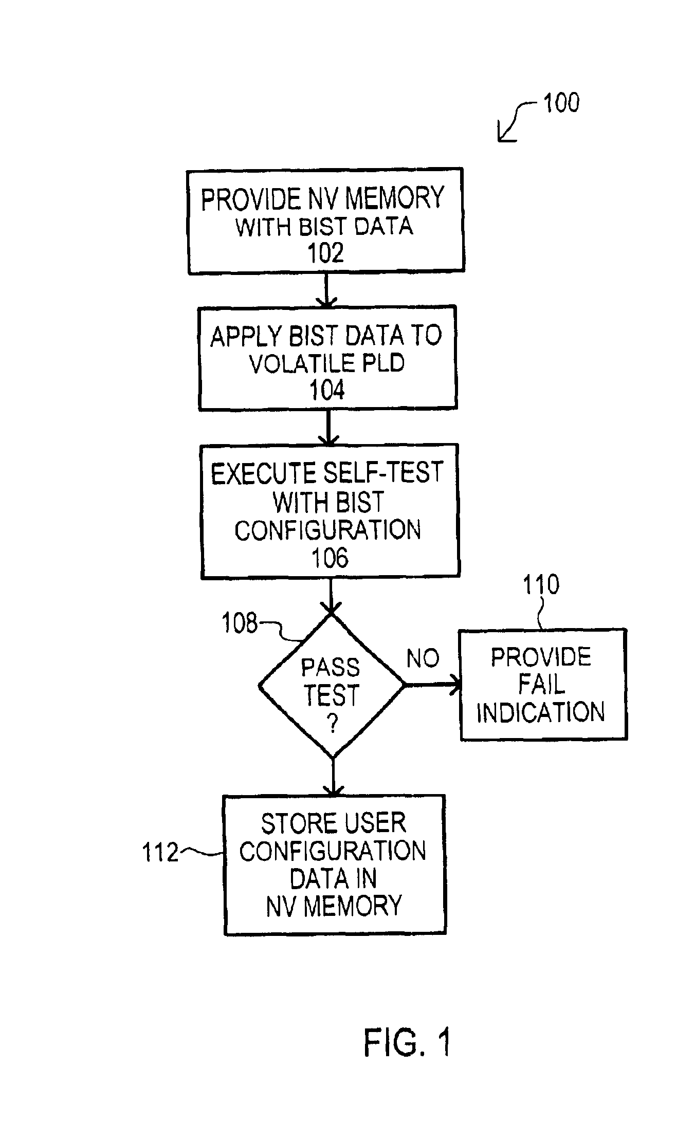
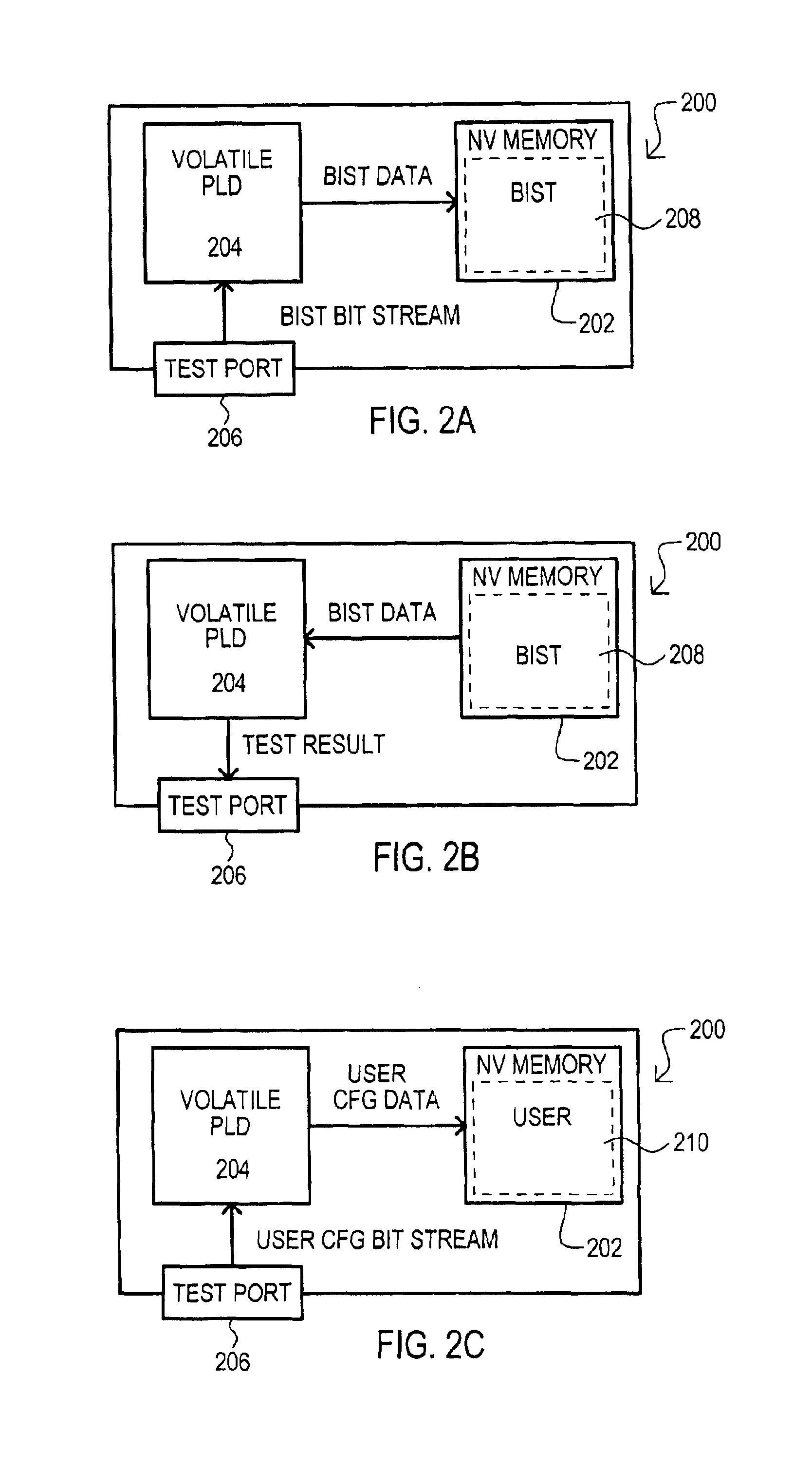
According to one embodiment, a programmable logic assembly (200) may include a nonvolatile memory (202) may be coupled to an associated volatile programmable logic device (PLD) (204). Built-in-self-test (BIST) data (208) may be stored in a nonvolatile memory (202) that places the volatile PLD (204) in a self-test configuration. If a volatile PLD (204) passes a self-test, user data (210) may be stored in a nonvolatile memory (202) that places a volatile PLD (204) into a user determined configuration.

Description

TECHNICAL FIELDThe present invention relates generally to programmable logic devices (PLDs), and more particularly to built-in-self-tests for PLDs.BACKGROUND OF THE INVENTIONProgrammable logic has increasingly become a valued resource for system designers. Programmable logic can allow for a custom logic design to be implemented without the initial cost, delay and complexity of designing and fabricating an application specific integrated circuit (ASIC).Currently, there are many variations of programmable logic, including simple programmable logic devices (SPLDs), complex PLDs (CPLDs), and field programmable gate arrays (FPGAs). Such devices typically include programmable logic circuits that operate in conjunction with corresponding memory circuits. The particular function of a logic circuit can be determined according to data stored in a corresponding memory circuit. Some programmable logic arrangements can include switching circuits (also called programmable interconnects) that can ...

Claims


Application Information

Patent Timeline
IPC IPC(8): G01R31/28G01R31/317G01R31/3185
CPCG01R31/31701G01R31/318516G01R31/31704
Inventor MOORE, MICHAEL T.
Owner CYPRESS SEMICON CORP
Learn More