Automatic bit fail mapping for embedded memories with clock multipliers

a clock multiplier and embedded memory technology, applied in the field of automatic bit fail mapping for embedded memories with clock multipliers, can solve the problems of generating a fail map with a low-speed ate tester that requires low-speed bist execution, and unable to keep up with on-chip clock speed, so as to achieve accurate bit fail mapping of embedded dram memory

Inactive Publication Date: 2005-06-02
IBM CORP
View PDF11 Cites 51 Cited by
  • Summary
  • Abstract
  • Description
  • Claims
  • Application Information

AI Technical Summary

Benefits of technology

[0012] The present invention provides a system and method of automatic bit fail mapping of embedded memories such as DRAM arrays on a chip while using a low-speed, off-chip ATE tester by running BIST test circuitry on the chip from an internal high-speed clock that is a multiplied frequency of the low-speed ATE tester clock. The ability to accurately bit fail map an embedded D...

Problems solved by technology

Automated Test Equipment (ATE) that can keep pace with on-chip clock speeds is becoming prohibitively expensive, rendering the capital investment necessary to provide at-speed test results undesirable.
Up to now, generating a Fail Map with a low-speed ATE tester required low-speed BIST execution, because ...

Method used


Image

  • Automatic bit fail mapping for embedded memories with clock multipliers
  • Automatic bit fail mapping for embedded memories with clock multipliers
  • Automatic bit fail mapping for embedded memories with clock multipliers

Examples


Embodiment Construction

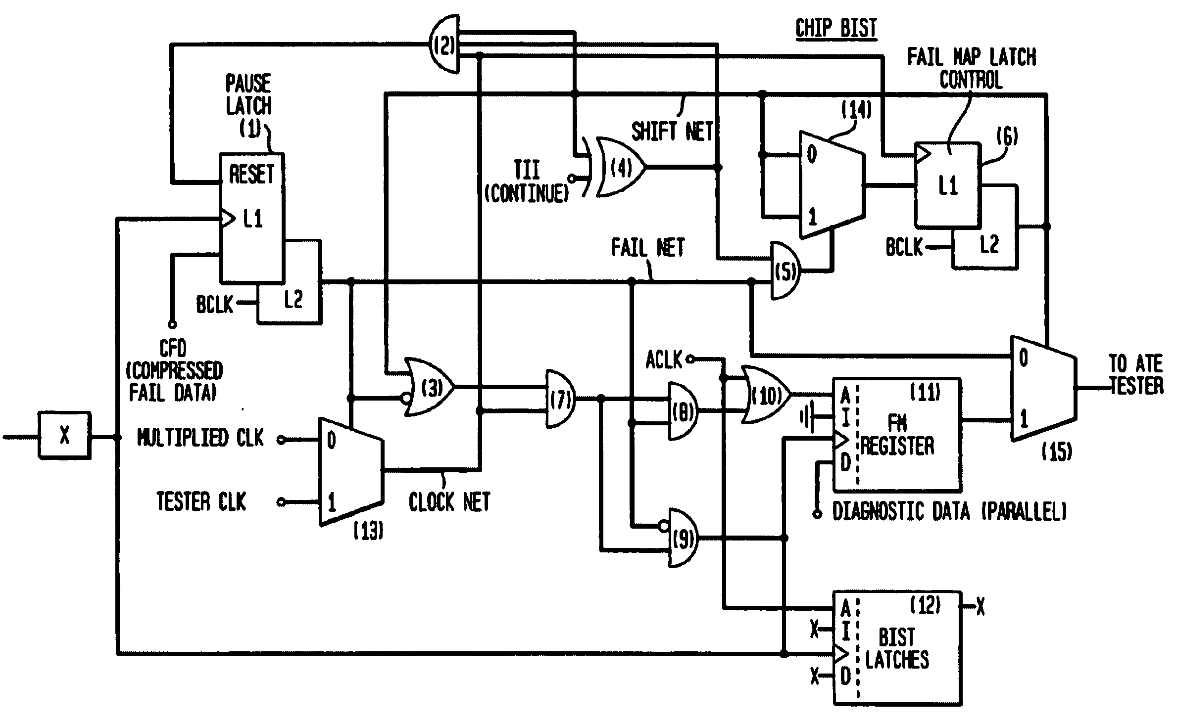
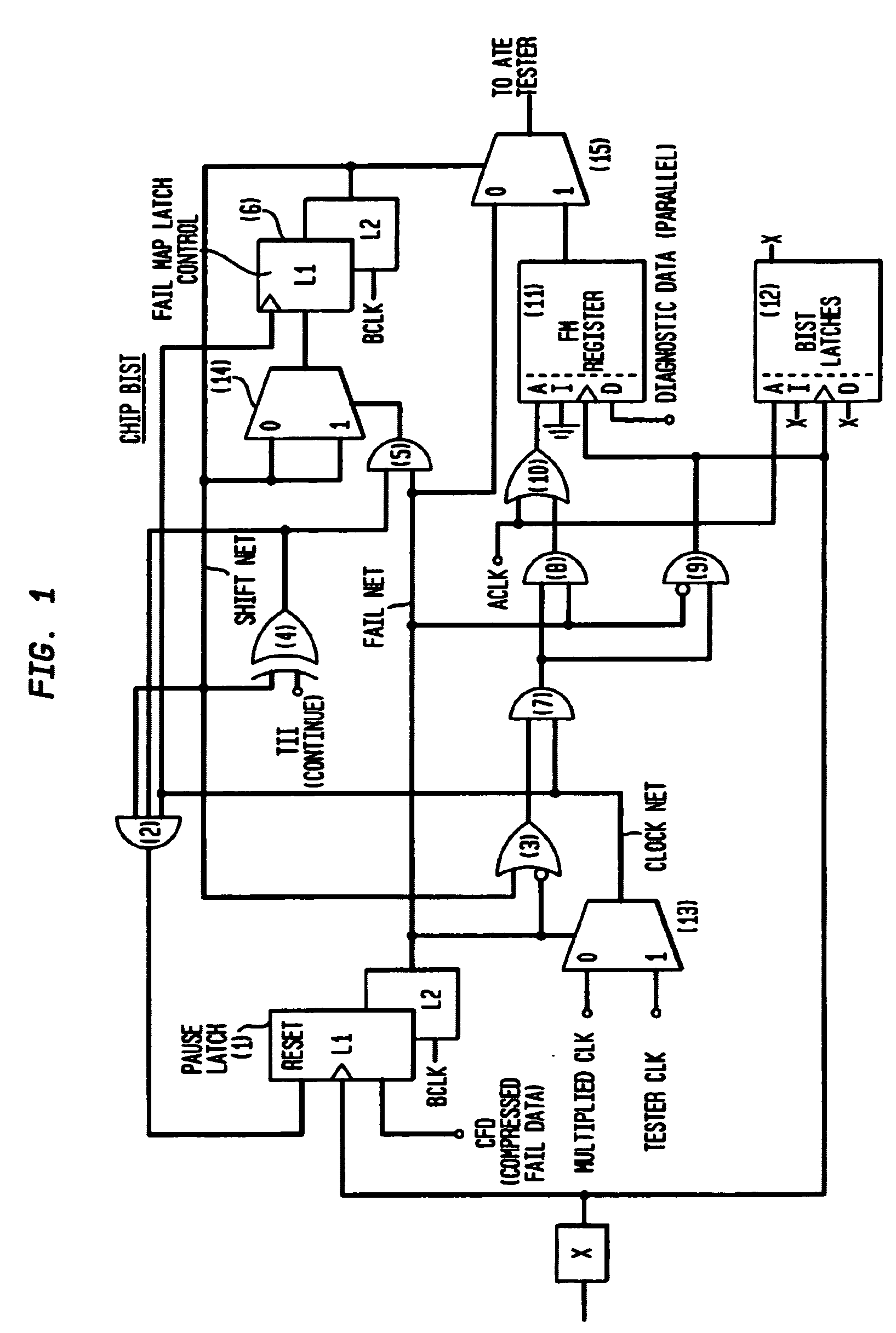
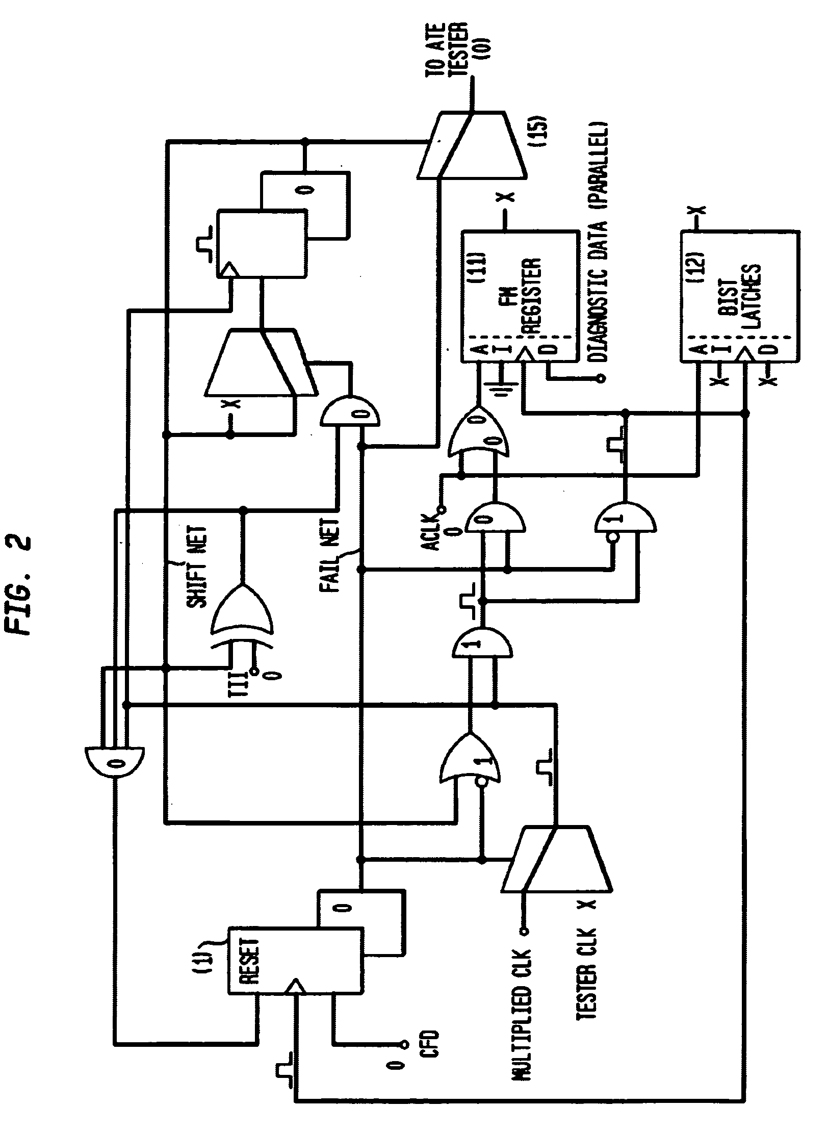
[0023] The present invention provides a methodology and a circuit wherein a BIST test engine is run off an internal multiplied clock until the occurrence of a fail, at which time the BIST and related test circuitry are paused until an ATE test acknowledgement automatically switches the BIST test circuitry to the ATE tester clock to guarantee that all bit fail location information shift out operations are synchronized between the ATE tester and the embedded test circuitry.

[0024] During test, the embedded memory is run off an internal multiplied clock that can be out of phase from the tester supplied ATE clock. The circuit and methodology of the present invention provide for accurate bit fail mapping, irrespective of the internal clock phase and multiplication factor.

[0025] The ATE tester is only required to produce a free running oscillating clock which is multiplied, and a BIST engine running off the multiplied clock stimulates the memory. As soon as a fail occurs, namely a mismat...


PUM


Abstract

A bit fail map circuit accurately generates a bit fail map of an embedded memory such as a DRAM by utilizing a high speed multiplied clock generated from a low-speed Automated Test Equipment (ATE) tester. The circuit communicates between the ATE tester, the embedded memory under test, Built-In Self-Test (BIST) and Built-In Redundancy Analysis (BIRA). An accurate bit fail map of an embedded DRAM memory is provided by pausing the BIST test circuitry at a point when a fail is encountered, namely a mismatch between BIST expected data and the actual data read from the array, and then shifting the bit fail data off the chip using the low-speed ATE tester clock. Thereafter, the high-speed test is resumed from point of fail by again running the BIST using the high-speed internal clock, to provide at-speed bit Fail Maps.

Description

BACKGROUND OF INVENTION [0001] 1. Field of the Invention [0002] The present invention relates generally to automatic bit fail mapping for embedded memories with clock multipliers, and more particularly pertains to automatic bit fail mapping for embedded DRAMs (Dynamic Random Access Memories) with clock multipliers. [0003] More specifically, a system and method are provided of automatic bit fail mapping of embedded memories such as DRAM arrays on a chip while using a low-speed, off-chip ATE (Automatic Test Equipment) tester. BIST (Built In Self Test) test circuitry on the chip is run from an internal high-speed clock that is a multiplied frequency of the low-speed ATE tester clock. An accurate bit fail map of an embedded DRAM memory is provided by stopping the BIST test circuitry at a point when a fail is encountered, namely a mismatch between BIST expected data and the actual data read from the array, and then shifting the bit fail data off the chip using the low-speed ATE tester cl...

Claims


Application Information

Patent Timeline
IPC IPC(8): G06F11/00G11C29/00G11C29/14G11C29/56
CPCG11C29/14G11C2029/5604G11C29/56008G11C29/56
Inventor ANAND, DARREN L.GORMAN, KEVIN W.NELMS, MICHAEL R.
Owner IBM CORP
Why Eureka
Try Eureka