Electrical connection device

a technology of electrical connection and connection device, which is applied in the direction of coupling device connection, sustainable manufacturing/processing, final product manufacturing, etc., can solve the problems of easy distortion and damage during replacement, limited contact area, and poor electrical characteristi

Inactive Publication Date: 2004-02-17
VIA TECH INC
View PDF8 Cites 81 Cited by
  • Summary
  • Abstract
  • Description
  • Claims
  • Application Information

AI Technical Summary

Problems solved by technology

Since the pin 111 is not hard and still enough, it is easy to be distorted and damaged during replacement.
The contact area is limited, the electrical characteristic is bad and the intensity of the structure of the combination is weaker.
The disadvantages lead the rising of the defects of the products and sometimes the department of the solder ball 138.
Also, the overflow of the solder ball 138 will lead the circuit shortage and the electrical instability.
In the same time the disadvantage also includes the bad co-planarity between the electrical connection device 13a and the main board 12a.

Method used


Image

  • Electrical connection device
  • Electrical connection device
  • Electrical connection device

Examples


Embodiment Construction

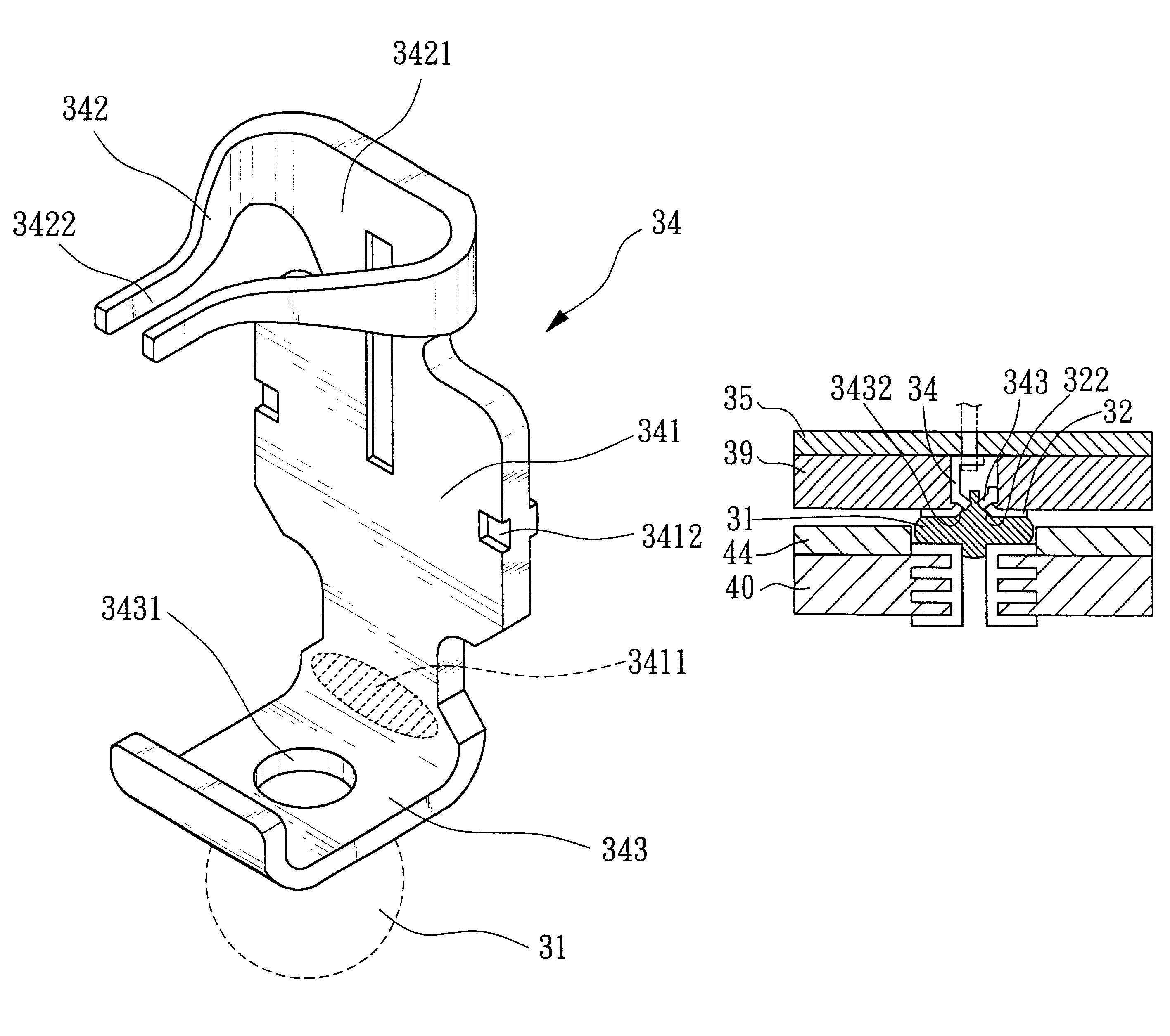
The major feature of the present invention is to enlarge the contact area of the solder ball and the socket by the suitable design of the geometrical structure after the solder reflow process. The contact area between the bottom part of the socket and the solder ball can be produced as the difference in height of the concave and convex part of the solder pad on the bottom part of the electrical conducting metal or can be the holes or the slope. Or, an extra contact ring in the area of the solder pad can be added optionally. The contact area also can be enlarged by the different height between the contact ring and the solder pad by the design of the geometrical structure. Part of the solder ball will flow into the convex and concave part of the solder pad, the hole and the slope in the solder reflow process to achieve the coupling effect. Enlarged contact area will also improve the electrical characteristics, the intensity of the structure and the yield of the product.

The following e...


PUM


Abstract

An electrical connection device comprises a socket, a plurality of electrical conducting holder in between, a contact ring and a plurality of solder balls. A plurality of pin holes are placed on the socket to provide the insert function for the pins of a IC package. The electrical conducting holder is placed in the pin holes and comprises an extensional part, a holder on the top of the extension part and a solder pad on the bottom part of the extension part to combine the solder ball. At least one 2D or 3D geometrical structure such as the hole, the convex and concave part or the slope on the bottom surface of the solder pad is formed. The geometrical structure will make the bottom surface of the solder pad not the flat plane. With the geometrical structure and the contact ring, the contact area of the solder pad and the contact ring will be enlarged during the solder reflow process. The coupling effect will be better and meanwhile improve the characteristics of the electricity, the intensity of the structure, the production yield and the characteristics of the co-planarity.

Description

(a) Field of the InventionThe present invention relates to an electrical connection device. Especially, the present invention relates to the structure improvement of the electrical connection device soldered on a main board by solder balls, wherein the device can be provided for inserting and placing an IC package.(b) Description of the Prior ArtFor long time, there are two ways that placing the Integrated Circuit (IC) Package on the Circuit Board (or Main Board). In one of the two ways, the IC is soldered fixedly on the main board and can not be removed. Another way the IC is replaceable. The replaceable electrical connecting device and the IC combining device are usually suitable in a IC package that needs upgrade sometimes or in a IC package with high price. In the case that one of the IC package broken and needs to be replaced, other packages can be kept. The best example is the socket and the circuit board connecting device that used for a Central Processing Unit (CPU).Please r...

Claims


Application Information

Patent Timeline
Patent Type & Authority Patents(United States)
IPC IPC(8): H05K3/34H05K1/18
CPCH01R9/091H01R12/57H05K3/3426H05K3/3436H01R12/716Y02P70/50
Inventor KUNG, MORISSHO, KWUN-YAO
Owner VIA TECH INC
Why Eureka
Try Eureka