Vacuum load lock, system including vacuum load lock, and associated methods

a vacuum load lock and vacuum load technology, applied in the field of vacuum load lock and vacuum load lock, can solve the problems of limiting the number of semiconductor wafers that can be produced with the semiconductor tool, and affecting the efficiency of the vacuum load lock

Inactive Publication Date: 2004-03-09
EDWARDS VACUUM LLC
View PDF24 Cites 14 Cited by
  • Summary
  • Abstract
  • Description
  • Claims
  • Application Information

AI Technical Summary

Problems solved by technology

Because the volume of the load locks are large, it can take several seconds or even minutes to cycle between atmospheric pressure and vacuum conditions.
This, in turn, limits the number of semiconductor wafers that can be produced with the semiconductor tool.
For example, typical through rates of semiconductor tools range between 100 to 150 semiconductor wafers per hour, and attempts to improve these rates are limited by the pressure cycling of the load locks.
In addition, these load locks often require large amounts of gas to be added or withdrawn quickly, which creates potential problems of damaging or contaminating the wafers.
Decreasing the size of the load lock, however, presents a number of technical challenges.

Method used


Image

  • Vacuum load lock, system including vacuum load lock, and associated methods
  • Vacuum load lock, system including vacuum load lock, and associated methods
  • Vacuum load lock, system including vacuum load lock, and associated methods

Examples


second embodiment

FIG. 6 is a schematic diagram showing the valving arrangement for the load lock system;

FIGS. 7A and 7B are schematic, partial cross-section views of a second embodiment of the object receiving mechanism, wherein FIG. 7A shows the object receiving mechanism in a lowered position, and FIG. 7B shows the object receiving mechanism in a raised position; and

FIG. 8 is a schematic diagram of a semiconductor tool system and processing chamber.

DESCRIPTION OF THE EMBODIMENTS

Reference will now be made in detail to exemplary embodiments of the invention, examples of which are illustrated in the accompanying drawings. Wherever possible, the same reference numbers will be used throughout the drawings to refer to the same or like parts.

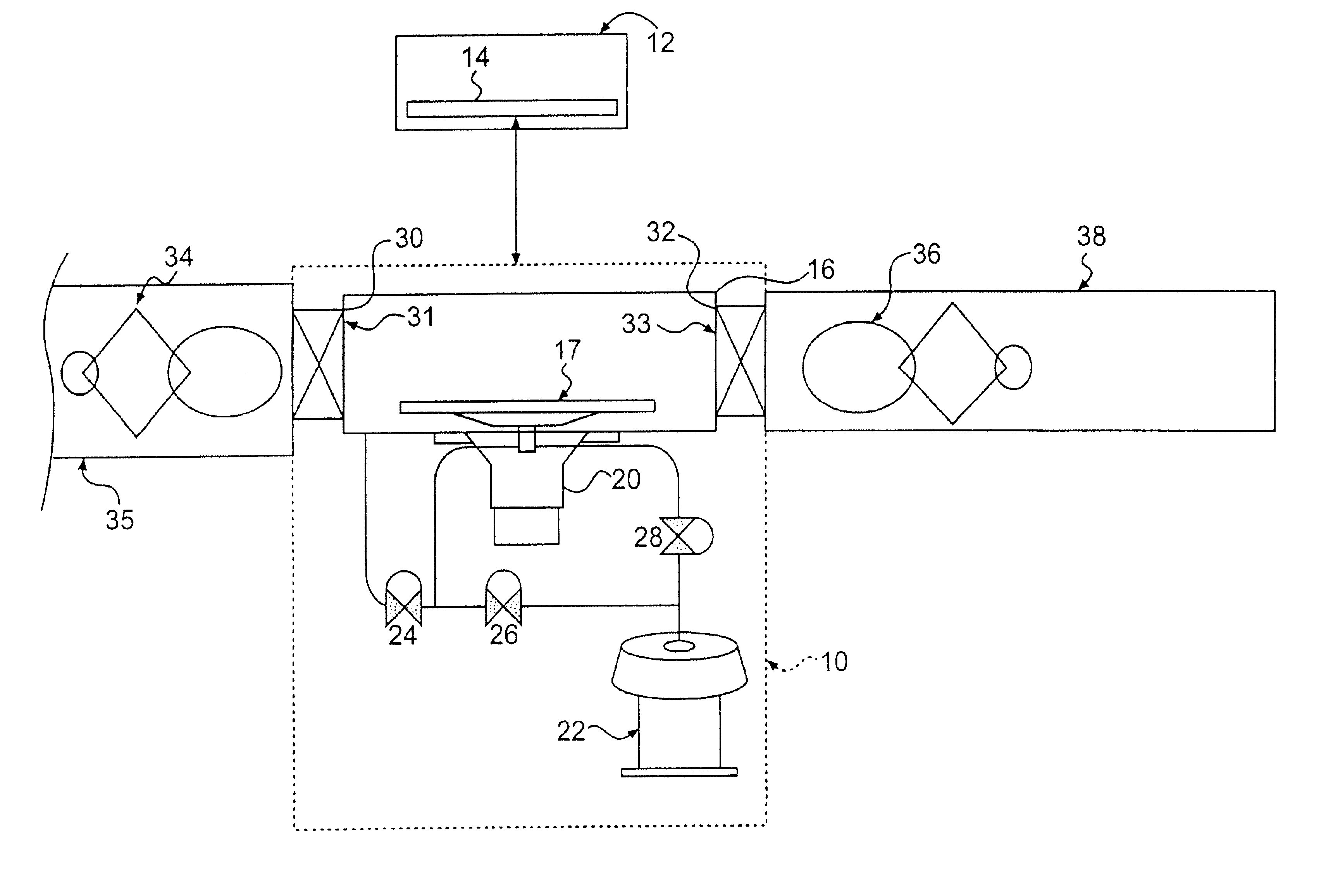
One embodiment of a load lock system including a load lock apparatus 10 of the present invention is shown in FIG. 1. The load lock apparatus 10 includes a chamber 16 defining an interior configured to receive an object 17. The object may be a substrate, such as, for ...

first embodiment

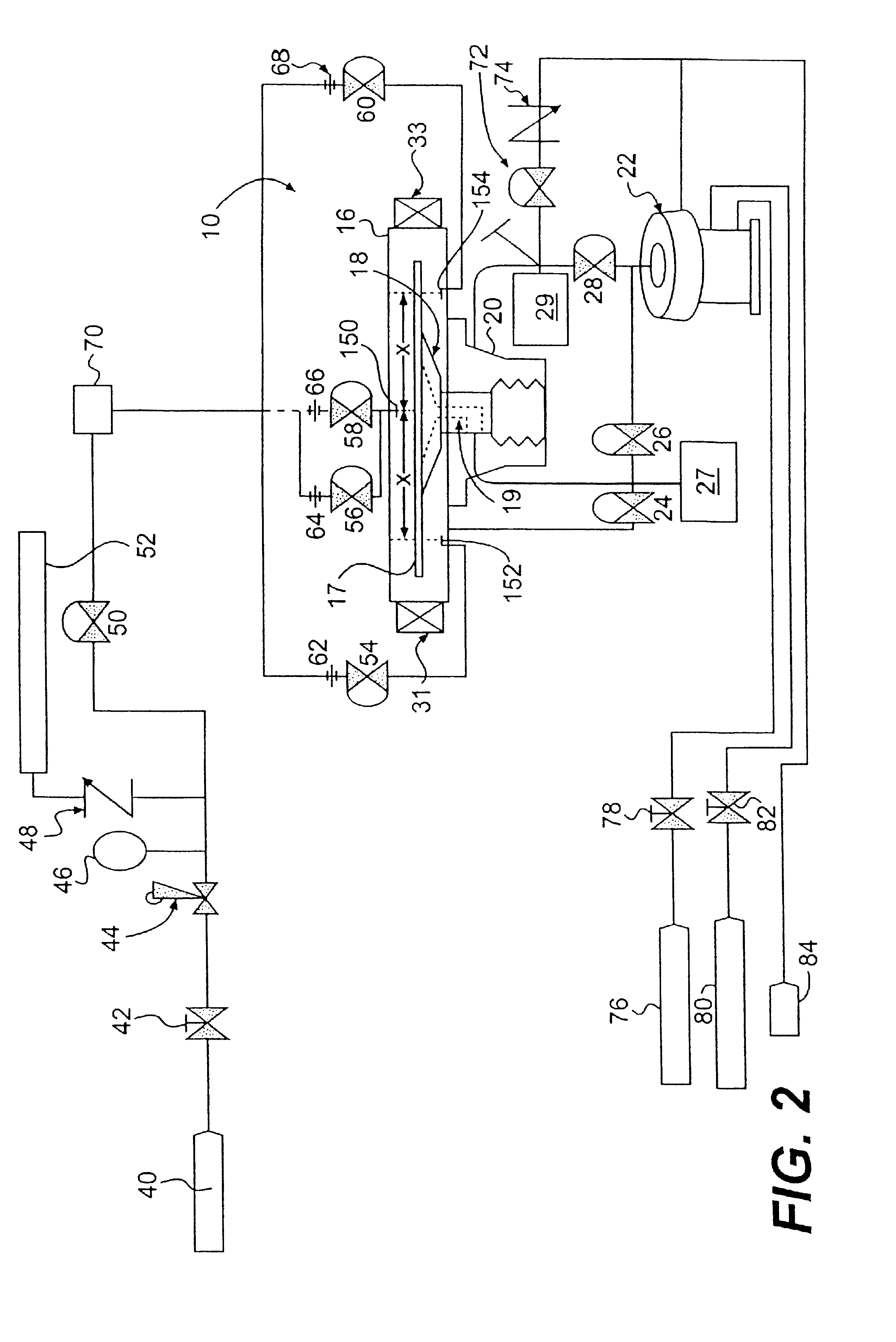
One exemplary embodiment of the load lock apparatus 10 suitable for use in the load lock system is shown in FIG. 4. The chamber 16 may have a volume sized to contain approximately 1.5 liters of gas and be configured to receive objects, such as substrates, having a maximum dimension (e.g., diameter, width, or diagonal distance) of approximately 200 mm to 300 mm. Alternatively, the chamber 16 could have any other size. For example, the chamber 16 could be sized to contain a volume of gas ranging from about 0.5 liters to about 10 liters; or from about 6 liters to about 10 liters; or from about 0.5 liters to about 1.5 liters; or less than about 10 liters, depending on the size and nature of the substrate.

The chamber 16 of the load lock apparatus 10 includes a lid 86 configured to provide access to the interior of the chamber 16 for maintenance or inspection. Located on the lid 86 is a plurality of heating elements 88 which may be used to keep the interior of the chamber 16 at a desired ...


PUM

PropertyMeasurementUnit
timeaaaaaaaaaa
timeaaaaaaaaaa
volumeaaaaaaaaaa

Abstract

A system is provided that includes a load lock apparatus having an interior configured to receive an object. At least one inlet valve may be flow coupled to the interior of the load lock apparatus, and at least one outlet valve may also be flow coupled to the interior of the load lock apparatus. A controller may be configured to selectively control opening and closing of the at least one inlet valve. The load lock apparatus may include an object receiving mechanism that is movable within the interior of the load lock apparatus to throttle the evacuation of the interior. Several methods of using the system and load lock apparatuses are also disclosed.

Description

DESCRIPTION OF THE INVENTION1. Field of the InventionThe present invention is generally directed to apparatuses, systems, and methods associated with substrate processing. Certain aspects of the present invention are directed to a load lock apparatus, systems, and methods useable in semiconductor wafer processing and / or processing of other substrates, such as those intended for flat panel displays. Other aspects may be related to processing chambers for substrate processing.2. Background of the InventionIn order to produce semiconductor wafers, manufactures start with an unprocessed substrate and perform various processing steps to convert the substrate to a semiconductor wafer. These process may include scrubbing the substrate to provide a clean surface, etching, depositing, or plating the substrate, and cooling the substrate to produce the finished semiconductor wafer. Some of these steps may be grouped together and performed within a single semiconductor tool.A semiconductor tool...

Claims


Application Information

Patent Timeline
Patent Type & Authority Patents(United States)
IPC IPC(8): B24B37/04G03F7/20H01L21/00B24B37/34B65G49/07
CPCB24B37/345G03F7/7075G03F7/70808G03F7/70841H01L21/67253Y10S414/135
Inventor DICKINSON, COLIN JOHNMURPHY, DAIMHIN PAUL
Owner EDWARDS VACUUM LLC
Why Eureka
Try Eureka