Electronic device and method for manufacturing the same, and method for shielding printed circuit board

a printed circuit board and electronic device technology, applied in the direction of flexible screening containers, coupling device connections, electrical apparatus construction details, etc., can solve the problems of not being widely used in general in respect of cost or availability, generating a big noise, and not being able to achieve the effect of suppressing the high frequency noise generated in the ground plane of the printed circuit board

Inactive Publication Date: 2004-03-16
KONICA CORP
View PDF6 Cites 23 Cited by
  • Summary
  • Abstract
  • Description
  • Claims
  • Application Information

AI Technical Summary

Benefits of technology

Further, another object of the present invention is to reduce a noise generated from a printed circuit board without making the printed circuit board high multi-layered so much.
According to the electronic device and the method for shielding the printed circuit board of the present invention, since the ground of the printed circuit board and the electromagnetic shielding layer or the electromagnetic shielding member are electrically conducted, the electromagnetic shielding layer or member functions not only as a shield for shielding an electromagnetic noise radiated from the printed circuit board but also as a ground layer. That is, the same effect as increasing one ground layer can be obtained. Therefore, a return path of signals from the wiring patterns of the printed circuit board can be obtained stably. Thus, the ground can be reinforced without making the printed circuit board high multi-layered.
Further, since the electrically insulating layer is sandwiched in between the printed circuit board and the electromagnetic shielding layer or member which functions as a ground layer, the capacity of the capacitor formed between the signal layer of the printed circuit board and the ground layer, between the power supply layer and the ground layer, or the like, becomes large. Thereby, the characteristic impedance of the printed circuit board lowers, and noises are absorbed by the whole printed circuit board. In particular, the noises (common mode noise and differential mode noise) generated between the power supply layer and the ground layer can be reduced well. Moreover, the capacity of the above-described capacitor can be made large, and the above-described return path can also be made short by adhering the electromagnetic shielding layer or member to at least one face of the printed circuit board through the electrically insulating layer. Therefore, noises can be further reduced.
Thus, noises, particularly the noises generated between the power supply layer and the ground layer can be reduced well without making the printed circuit board high multi-layered.

Problems solved by technology

Thereby, even though the printed circuit board is shielded, if this cable is connected to the outside of the shield, noises (there are two noises, a common mode noise such that the noises of the power supply and that of the ground are common mode, and a differential mode noise such that those noises appear in differential mode) appear in the power supply and the ground (GND) itself of the printed circuit board, and this cable will operate as an antenna and will generate a big noise.
That is, with the structure of such a shielding plate or a shielding member in earlier technology, the effect of suppressing the high frequency noise generated in the ground plane of a printed circuit board cannot be expected.
However, it is required to use a special material, so that it has not been used widely in general in respect of cost or availability.
Further, since the electrically insulating layer is sandwiched in between the printed circuit board and the electromagnetic shielding layer or member which functions as a ground layer, the capacity of the capacitor formed between the signal layer of the printed circuit board and the ground layer, between the power supply layer and the ground layer, or the like, becomes large.

Method used


Image

  • Electronic device and method for manufacturing the same, and method for shielding printed circuit board
  • Electronic device and method for manufacturing the same, and method for shielding printed circuit board
  • Electronic device and method for manufacturing the same, and method for shielding printed circuit board

Examples


first embodiment

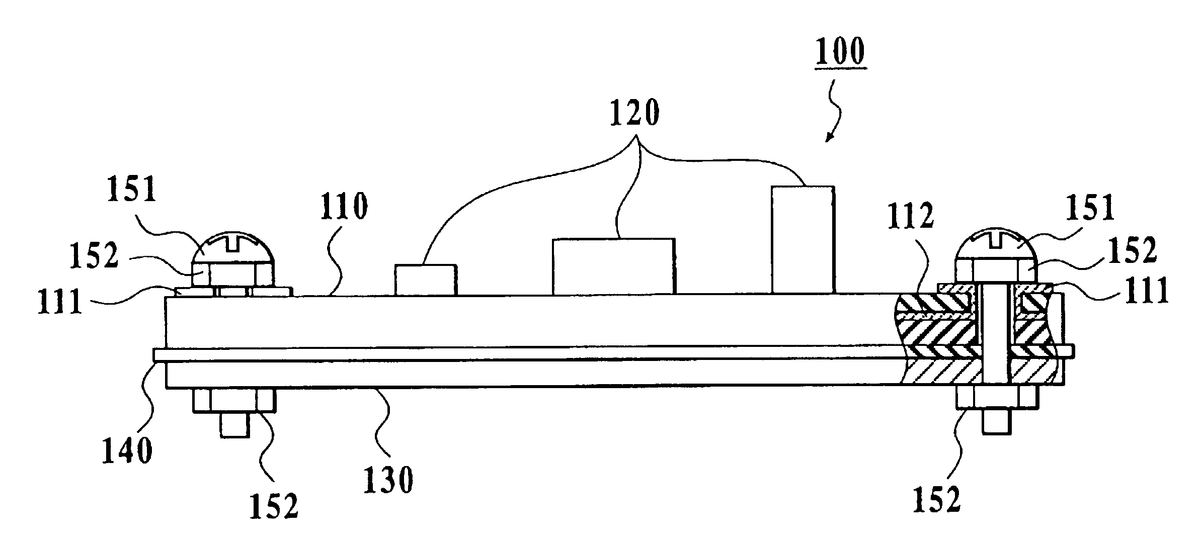
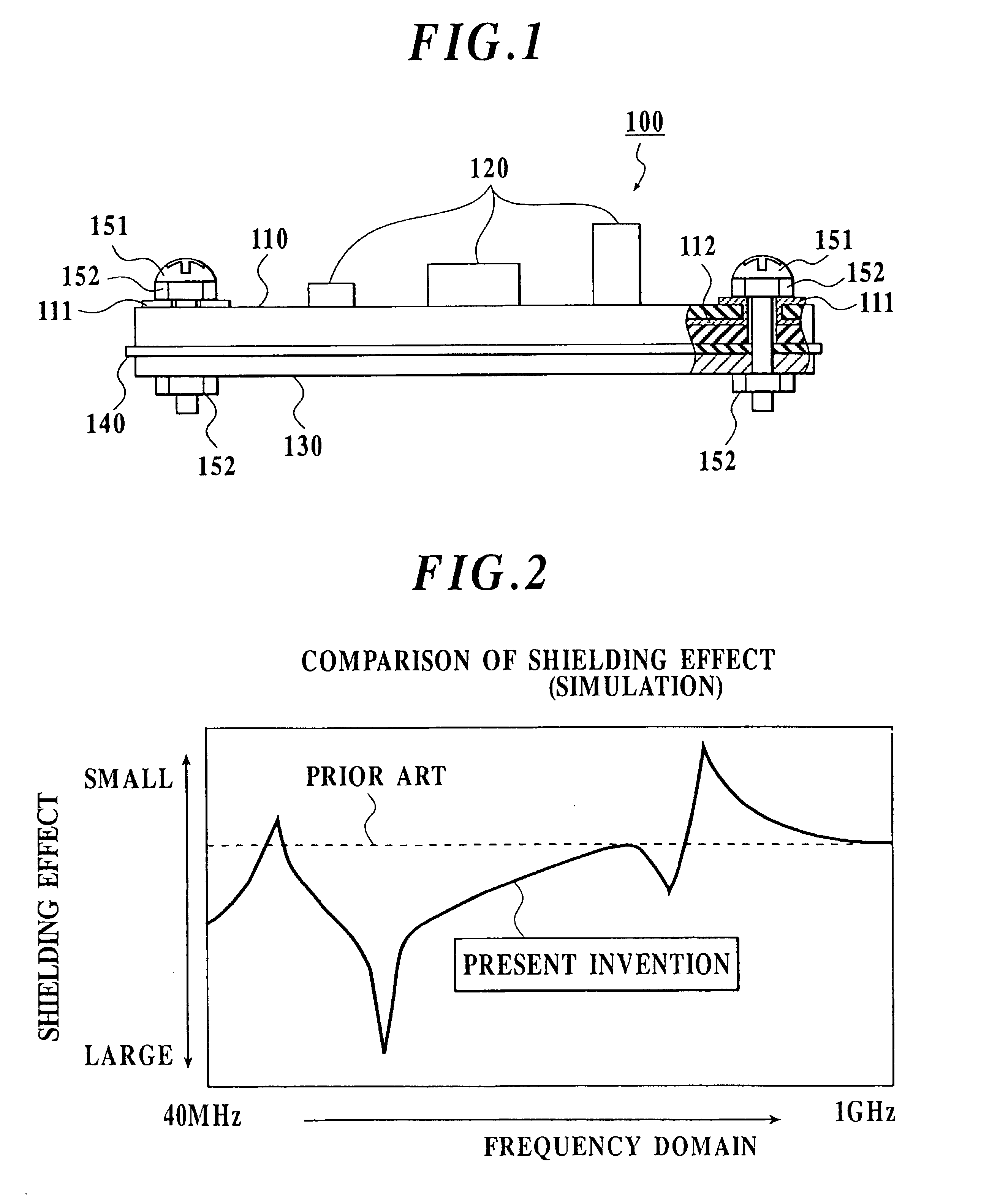
Hereinafter, the present invention will be explained with reference to FIG. 1.

In an electronic device 100 of the embodiment, as shown in FIG. 1, a shielding plate (electromagnetic shielding layer) 130 is adhered to a printed circuit board 110 through a thin insulating sheet (electrically insulating layer) 140. Moreover, in order to conduct electrically a ground pattern (ground) 111 of the printed circuit board 110 to the shielding plate 130 certainly, a resist in a portion of the ground pattern 111 is completely removed. The ground pattern 111 and the shielding plate 130 are tightened with bolts 151 and nuts 152, which are metal screws, so that they are electrically conducted completely. Therefore, the shielding plate 130 functions as a return path of signals which flow the wiring patterns (not shown) of the printed circuit board 110. Thereby, the same effect as increasing one layer of a ground layer of the printed circuit board 110 can be obtained. In addition, the reference numera...

second embodiment

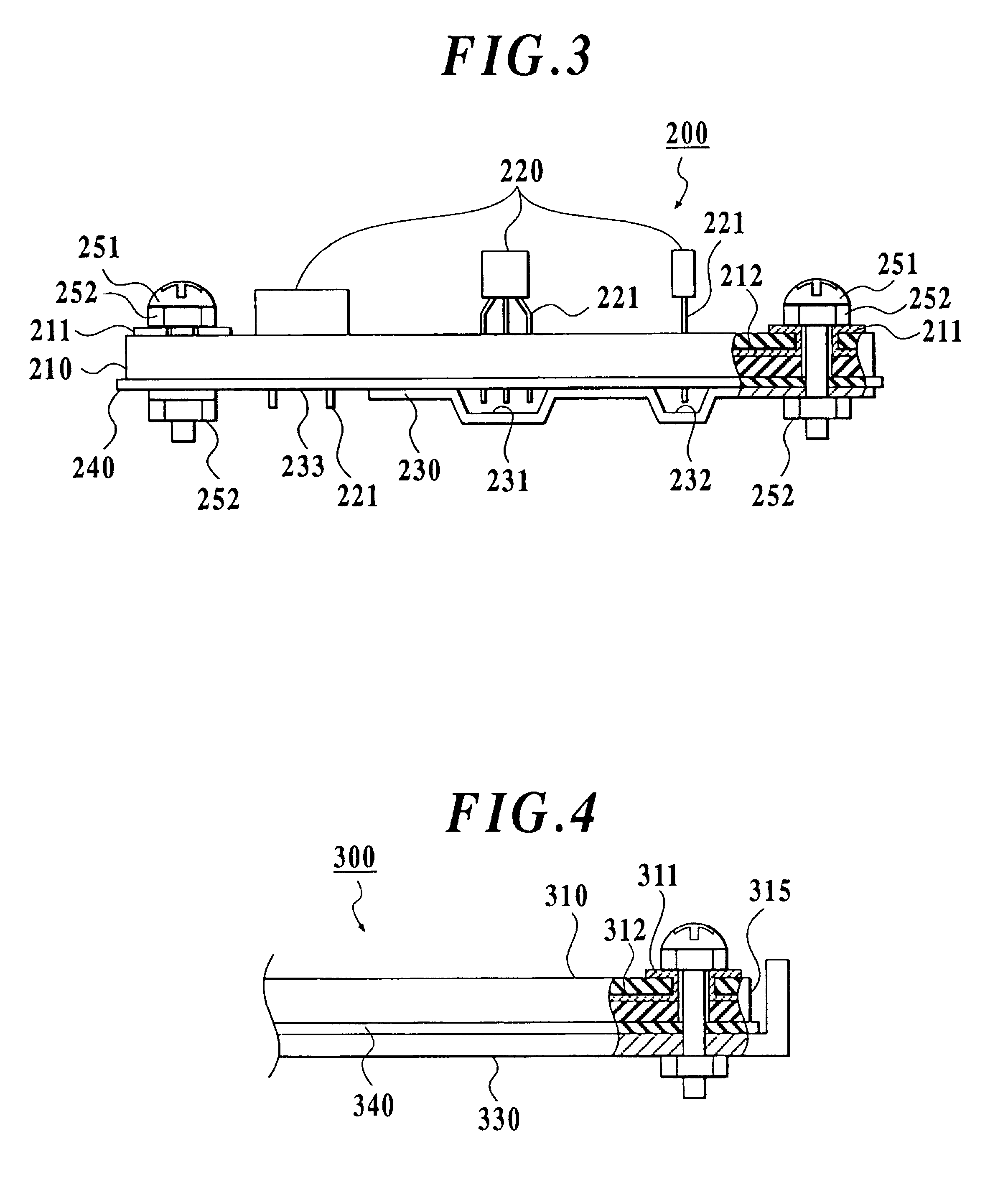
Next, the present invention will be explained with reference to FIG. 3.

In an electronic device 200 of the embodiment, as shown in FIG. 3, a shielding plate 230 provided with hollows 231 and 232 and a hole 233 is adhered to a printed circuit board 210 through an insulating sheet 240. The reason for providing the hollows 231 and 232 and the hole 233 is because unlike the case shown in FIG. 1, leads 221 of mounted electronic parts 220 may pass through the printed circuit board 210 or the insulating sheet 240 and may hit a shielding plate, when inserting the mounted electronic parts 220 in the printed circuit board 210. Thereby, the leads 221 provided on the electronic parts 220 for being mounted on the printed circuit board 210 will not be broken by hitting the shielding plate 230 even though the leads 221 pass through the printed circuit board 210 or the insulating sheet 240. Further, in the embodiment, since a ground pattern 211 of the printed circuit board 210 and the shielding plat...

third embodiment

Next, the present invention will be explained with reference to FIG. 4.

In an electronic device 300 of the embodiment, as shown in FIG. 4, a shielding plate 330 adhered to a printed circuit board 310 through an insulating sheet 340 has a shape of covering an end face 315 of the printed circuit board 310. Further, in the embodiment, a ground pattern 311 of the printed circuit board 310 and the shielding plate 330 are also electrically conducted through bolts 351 and nuts 352, which are metal screws. Thereby, the same effect as the above-described first and second embodiments can be obtained. Moreover, the electromagnetic noise can be prevented from radiating from the end face 315 of the printed circuit board 310. In particular, it has a great effect in preventing the radiation of the electromagnetic noise in a multi-layer printed circuit board. In addition, the reference numeral 312 in FIG. 4 indicates a ground plane of the printed circuit board 310.

Further, in the embodiment, the shi...


PUM


Abstract

An electronic device having a printed circuit board having a ground, an electrically insulating layer provided on a face of the printed circuit board, and an electromagnetic shielding layer adhered to the face of the printed circuit board through the electrically insulating layer. The ground of the printed circuit board and the electromagnetic shielding layer are conducted electrically.

Description

1. Field of the InventionThe present invention relates to an electronic device mounted with a printed circuit board, and a method for manufacturing the same. Moreover, the present invention relates to a method for shielding the printed circuit board in order to reduce electromagnetic noises radiated from the printed circuit board.2. Description of Related ArtIn earlier technology, in an electronic device mounted with a printed circuit board, as shown in FIG. 7A, a shielding plate 30 is disposed in only one face side of a printed circuit board 10, or as shown in FIG. 7B, a printed circuit board 20 is installed into a box-like shielding member 40 and all the six faces of the printed circuit board 20 are shielded. The shielding plate 30 and the shielding member 40 corresponding to the printed circuit boards 10 and 20, respectively, are used in order to prevent electromagnetic wave from radiating from the wiring patterns (not shown) in the printed circuit boards 10 and 20. The shielding...

Claims


Application Information

Patent Timeline
Patent Type & Authority Patents(United States)
IPC IPC(8): H05K9/00H05K1/02
CPCH05K1/0218H05K9/0022H05K9/0043
Inventor IGARASHI, YUTAKAKISHIMOTO, TADAO
Owner KONICA CORP
Why Eureka
Try Eureka