CMOS active pixel sensor with a sample and hold circuit having multiple injection capacitors and a fully differential charge mode linear synthesizer with skew control

a pixel sensor and sample and hold technology, applied in the field of cmos active pixel sensor systems, can solve the problems of pixel array b>101/b> not being calibrated to the same level, and affecting the uniformity of the imag

Inactive Publication Date: 2005-03-01
APTINA IMAGING CORP
View PDF7 Cites 31 Cited by
  • Summary
  • Abstract
  • Description
  • Claims
  • Application Information

AI Technical Summary

Problems solved by technology

An issue associated with the system 100 is that the pixels R, G, B of the pixel array 101 may not be calibrated to the same level.
These discrepancies are unwanted voltage offsets in the pixel signals, and have several adverse effects.
First, they distort the captured image.
For example, an image of an uniform field may not appear uniform due to variations in color and / or intensity.
Additionally, positive offsets may cause a reduction in the dynamic range of an image, due to a reduction in the useful ranges of voltages presented to the analog-to-digital converter 106.
Similarly, negative offsets may cause clipping.
Frequently, pixels sensitive to the same color may exhibit similar unwanted voltage offsets.
However, digital correction is problematic because correction in the digital domain utilizes valuable processing resources in an imaging system.
Additionally, correction in the digital domain does not address dynamic range reduction in the analog processing portion.

Method used


Image

  • CMOS active pixel sensor with a sample and hold circuit having multiple injection capacitors and a fully differential charge mode linear synthesizer with skew control
  • CMOS active pixel sensor with a sample and hold circuit having multiple injection capacitors and a fully differential charge mode linear synthesizer with skew control
  • CMOS active pixel sensor with a sample and hold circuit having multiple injection capacitors and a fully differential charge mode linear synthesizer with skew control

Examples


Embodiment Construction

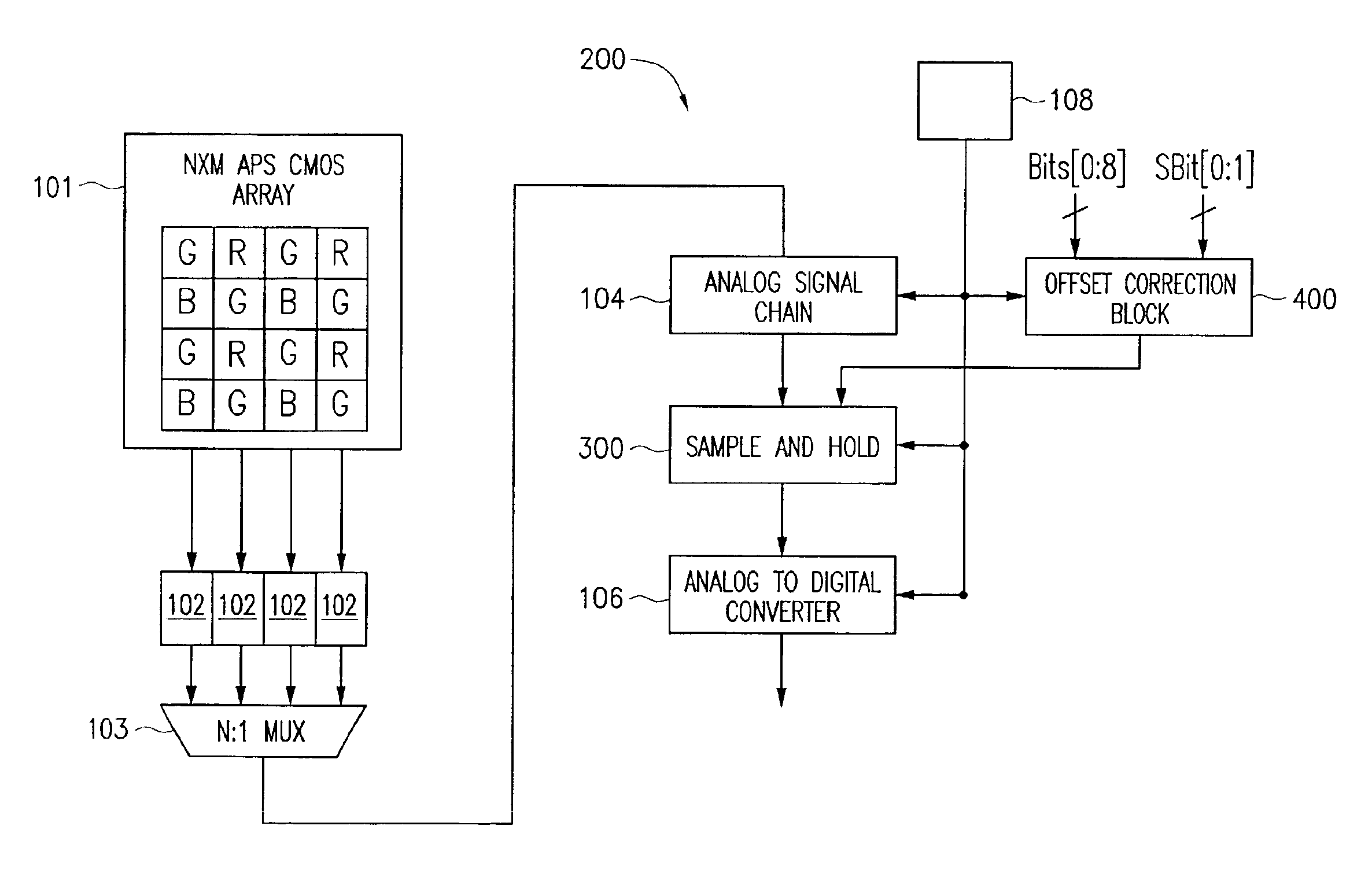
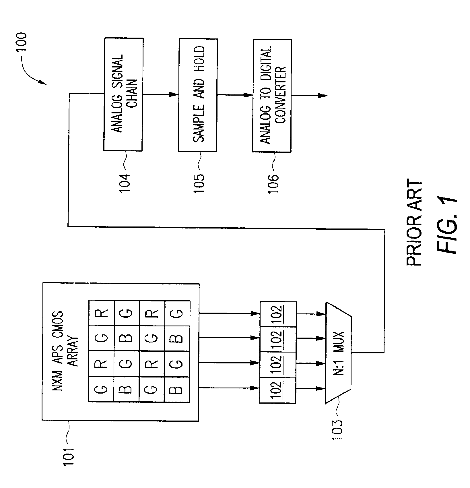
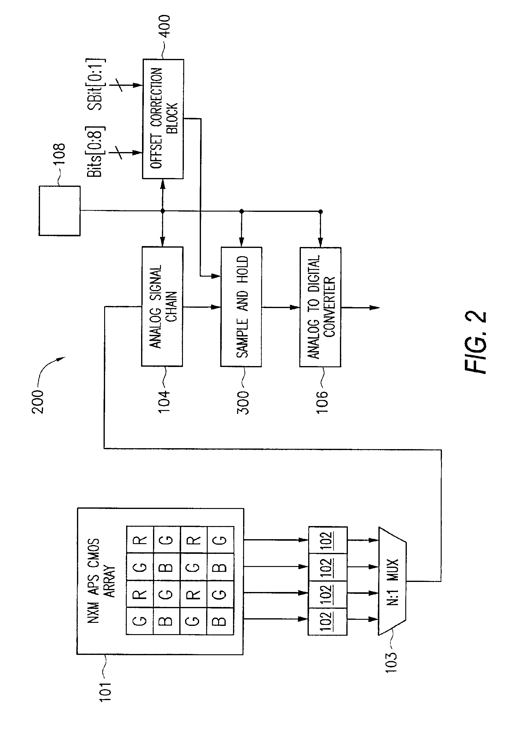
Now referring to the drawings, where like reference numerals designate like elements, there is shown in FIG. 2 a block diagram of an APS system 200 which is capable of applying per-color correction values to the output of the pixel array 101. The system 200 shares several components with the CMOS APS system 100 of FIG. 1. For example, both systems 100 and 200 includes a N×M APS CMOS array 101 comprising an array of pixels R, G, B, which are coupled to a row of pixel buffers 102. The output of the pixels R, G, B, i.e., a differential pixel signal comprising a reset signal component and a photo signal component, are transferred one row at a time from the pixel array 101 to the row of pixel buffers 102. The N:1 multiplexer 103 transfers the signals stored in one of the pixel buffers 102 at a time for further processing through an analog signal chain 104, a sample-and-hold circuit 300, and a analog-to-digital converter 106. System 200 also includes several new components. Digital correc...


PUM


Abstract

An CMOS active pixel sensor (APS) imaging system include circuitry to compensate for different analog offset levels from the CMOS pixel array. More specifically, the compensation is performed in the analog (charge) domain. A digital correction value, which may be measured as part of the operation or testing of the CMOS APS system, is provided to a offset correction block circuit, to generate an analog electrical signal. The analog electrical signal is supplied to a sample-and-hold circuit including a charge amplifier. The signal read from the pixel array, after conditioning through an analog signal chain, is also supplied to the charge amplifier, which has a linear transfer function and outputs the compensated signal.

Description

FIELD OF INVENTIONThe present invention relates to CMOS active pixel sensor systems. More specifically, the present invention relates to an apparatus and method for implementing analog offset correction in a CMOS active pixel sensor system.BACKGROUND OF THE INVENTIONFIG. 1 is an illustration of a color CMOS active pixel sensor (APS) system 100. The system 100 includes a N×M pixel array 101 comprised of pixels R, G, B respectively sensitive to red, green, and blue colored light. The pixels R, G, B are arranged in a Bayer pattern to model the human visual response. In the Bayer pattern, alternating rows are comprised of green / red and green / blue pixels. Any image focused upon the pixel array causes the pixels to convert the incident light into electrical voltages. Conventionally, each pixel outputs two signals including a reset signal corresponding to a base line voltage level, as well as a photo signal corresponding to the base line voltage level as modified by charge accumulation in ...

Claims


Application Information

Patent Timeline
Patent Type & Authority Patents(United States)
IPC IPC(8): H04N5/217H04N5/357H04N5/374H04N5/378
CPCH04N5/378H04N5/3653H04N25/672H04N25/75
Inventor ROSSI, GIUSEPPE
Owner APTINA IMAGING CORP
Why Eureka
Try Eureka