Micromirrors and off-diagonal hinge structures for micromirror arrays in projection displays

a technology of projection display and micromirror array, which is applied in the field of spatial light modulator fabrication with hinge structure, can solve the problems of short cathode life, low light efficiency of devices, and use of bulky and expensive vacuum tubes

Inactive Publication Date: 2005-03-15
VENTURE LENDING & LEASING IV +1
View PDF15 Cites 63 Cited by
  • Summary
  • Abstract
  • Description
  • Claims
  • Application Information

AI Technical Summary

Problems solved by technology

A disadvantage of the Eidophor system is that the oil film is polymerized by constant electron bombardment and oil vapors result in a short cathode lifetime.
A disadvantage of both of these systems is their use of bulky and expensive vacuum tubes.
Although the switching voltage of this SLM is lowered by connecting the deflectable mirror elements at only one corner, the device has low light efficiency due to the small fractional active area.
In addition, diffraction from the addressing circuitry lowers the contrast ratio (modulation depth) of the display.
If this distance is one-quarter of a wavelength, light directly reflected from the two surfaces will interfere destructively and the device will act as a diffraction grating, sending light into diffracted orders.
When the ribbons are deflected past a certain point, the restoring mechanical force can no longer balance the electrostatic force and the ribbons snap to the substrate.
However, there are several difficulties with the GLV.
A problem is that a passive addressing scheme might not be able to provide high frame rates (the rate at which the entire SLM field is updated).
This reduces the achievable contrast ratio.
Also, even though the device is substantially planar, light is scattered, as in the DMD, from areas between the pixels, further reducing the contrast ratio.
However, the device, being based on the birefringence of liquid crystals, requires polarized light, reducing its optical efficiency.
Furthermore, the response time of liquid crystals is slow.
This arrangement leads to expensive optical systems.

Method used


Image

  • Micromirrors and off-diagonal hinge structures for micromirror arrays in projection displays
  • Micromirrors and off-diagonal hinge structures for micromirror arrays in projection displays
  • Micromirrors and off-diagonal hinge structures for micromirror arrays in projection displays

Examples


Embodiment Construction

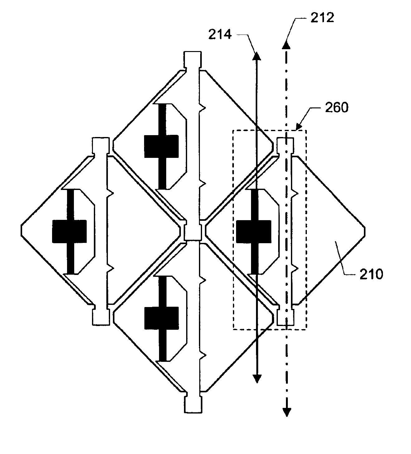
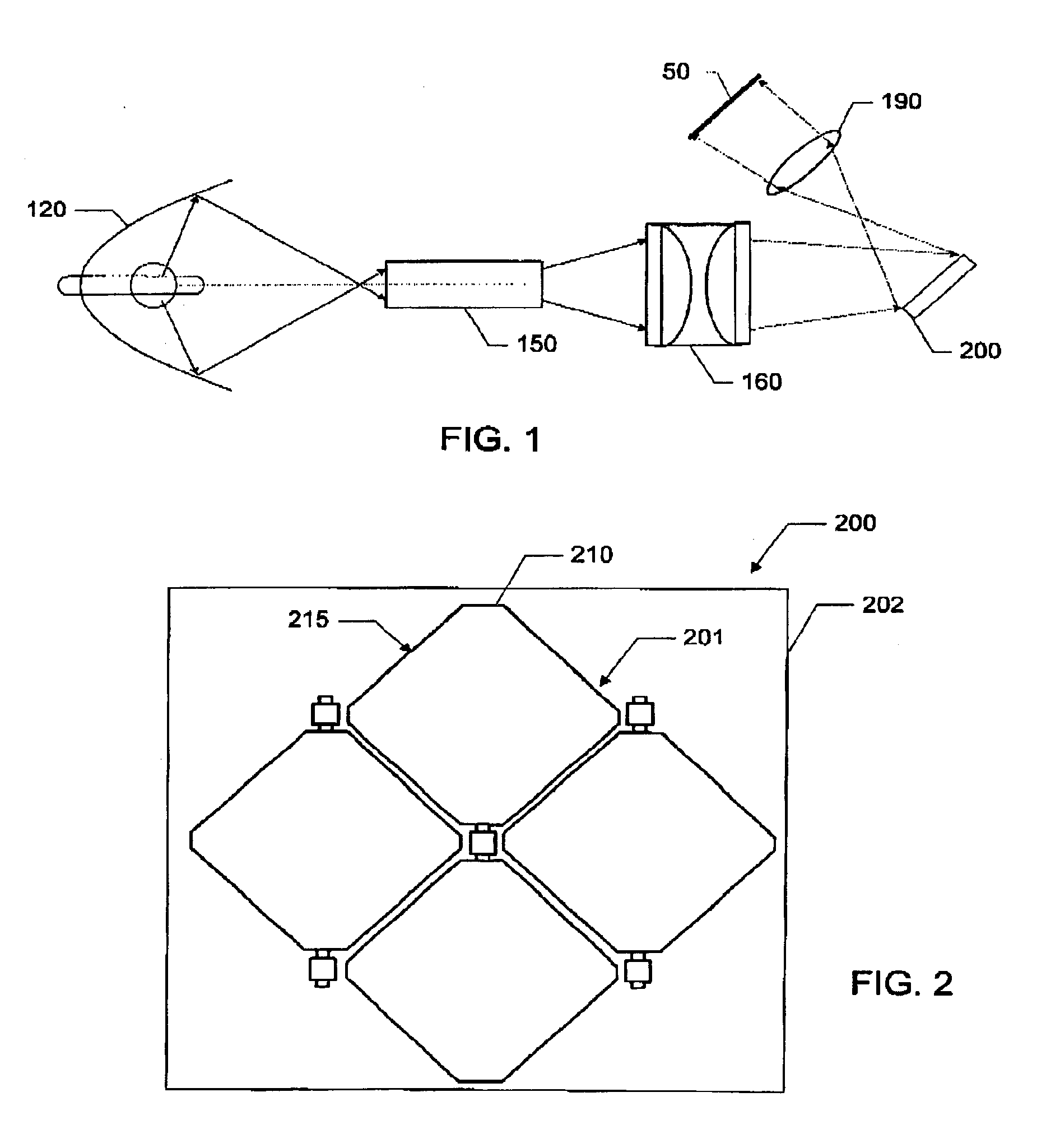
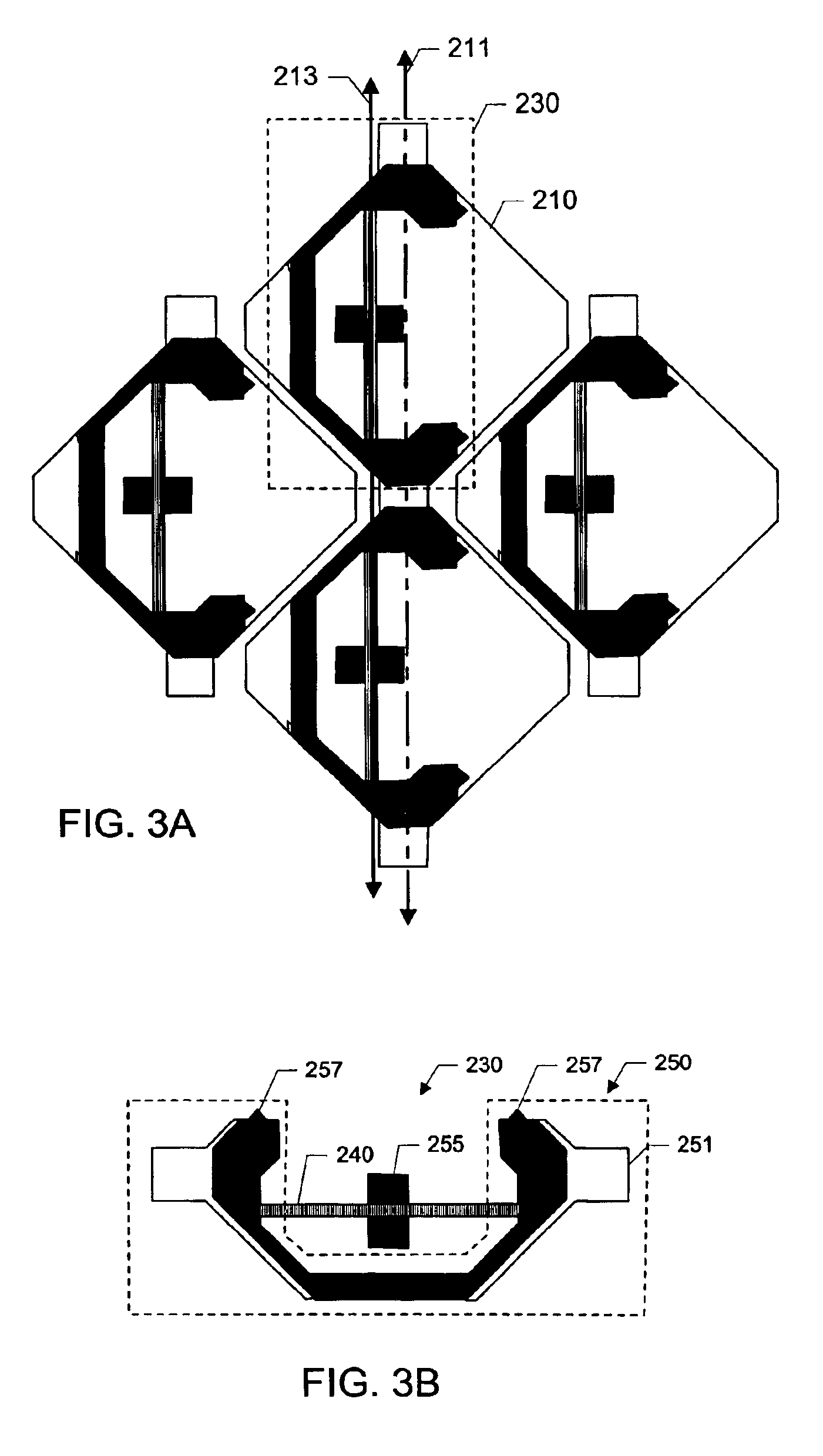
Processes for micro-fabricating a MEMS device such as a movable micromirror and mirror array are disclosed in U.S. Pat. Nos. 5,835,256 and 6,046,840 both to Huibers, the subject matter of each being incorporated herein by reference. A similar process for forming MEMS movable elements (e.g. mirrors) on a wafer substrate (e.g. a light transmissive substrate or a substrate comprising CMOS or other circuitry) is illustrated in the present application. By “light transmissive”, it is meant that the material will be transmissive to light at least in operation of the device (The material could temporarily have a light blocking layer on it to improve the ability to handle the substrate during manufacture, or a partial light blocking layer for decreasing light scatter during use. Regardless, a portion of the substrate, for visible light applications, is preferably transmissive to visible light during use so that light can pass into the device, be reflected by the mirrors, and pass back out of...


PUM

PropertyMeasurementUnit
angleaaaaaaaaaa
angleaaaaaaaaaa
diagonal lengthaaaaaaaaaa

Abstract

A spatial light modulator is disclosed, along with methods for making such a modulator, that comprises an array of micromirrors each having a hinge and a micromirror plate held via the hinge on a substrate, the micromirror plate being disposed in a plane separate from the hinge and having a diagonal extending across the micromirror plate, the micromirror plate being attached to the hinge such that the micromirror plate can rotate along a rotation axis that is parallel to, but off-set from the diagonal of the micromirror plate. Also disclosed is a projection system that comprises such a spatial light modulator, as well as a light source, condensing optics, wherein light from the light source is focused onto the array of micromirrors, projection optics for projecting light selectively reflected from the array of micromirrors onto a target, and a controller for selectively actuating the micromirrors in the array.

Description

TECHNICAL FIELD OF THE INVENTIONThe present invention is related generally to spatial light modulators, and, more particularly, to fabrications of spatial light modulators with hinge structures.BACKGROUND OF THE INVENTIONSpatial light modulators (SLMs) are transducers that modulate an incident beam of light in a spatial pattern in response to an optical or electrical input. The incident light beam may be modulated in phase, intensity, polarization, or direction. This modulation may be accomplished through the use of a variety of materials exhibiting magneto-optic, electro-optic, or elastic properties. SLMs have many applications, including optical information processing, display systems, and electrostatic printing.An early SLM designed for use in a projection display system is described by Nathanson, U.S. Pat. No. 3,746,911. The individual pixels of the SLM are addressed via a scanning electron beam as in a conventional direct-view cathode ray tube (CRT). Instead of exciting a phosp...

Claims


Application Information

Patent Timeline
Patent Type & Authority Patents(United States)
IPC IPC(8): G03B21/28G02B7/182G02B26/08
CPCG03B21/28G02B26/0841B81B7/0067B81B7/04
Inventor PATEL, SATYADEV R.HUIBERS, ANDREW G.
Owner VENTURE LENDING & LEASING IV
Why Eureka
Try Eureka