Stack package using flexible double wiring substrate

a technology of stacking and wiring substrate, which is applied in the direction of semiconductor devices, semiconductor/solid-state device details, electrical apparatus, etc., can solve the problems of increasing failure rates, low failure rate of stacking package, and limited size of printed circuit boards

Inactive Publication Date: 2005-04-05
SAMSUNG ELECTRONICS CO LTD
View PDF10 Cites 127 Cited by
  • Summary
  • Abstract
  • Description
  • Claims
  • Application Information

AI Technical Summary

Benefits of technology

It is further desirable to provide a stack package manufactured by the conventional CSP manufacturing process using the tape circuit board.

Problems solved by technology

Thus, the BGA package improves the mounting density on the motherboard but is limited by the size of the printed circuit board.
Since a stack package using the conventional semiconductor packages employs packages that have already passed reliability tests, the stack package has a low failure rate but is comparatively thick.
The stack chip package, however, employs chips that were not previously inspected in reliability tests, thereby increasing failure rates.
However, it is not easy to stack the CSPs, each of which is mounted on the printed circuit board.
That is, since the conventional CSP contains only solder bumps formed on the upper surface of the tape circuit board for external connection terminals, it is difficult to three-dimensionally stack the conventional CSPs.

Method used


Image

  • Stack package using flexible double wiring substrate
  • Stack package using flexible double wiring substrate
  • Stack package using flexible double wiring substrate

Examples


Embodiment Construction

Preferred embodiments of the present invention will be described below with reference to the accompanying drawings.

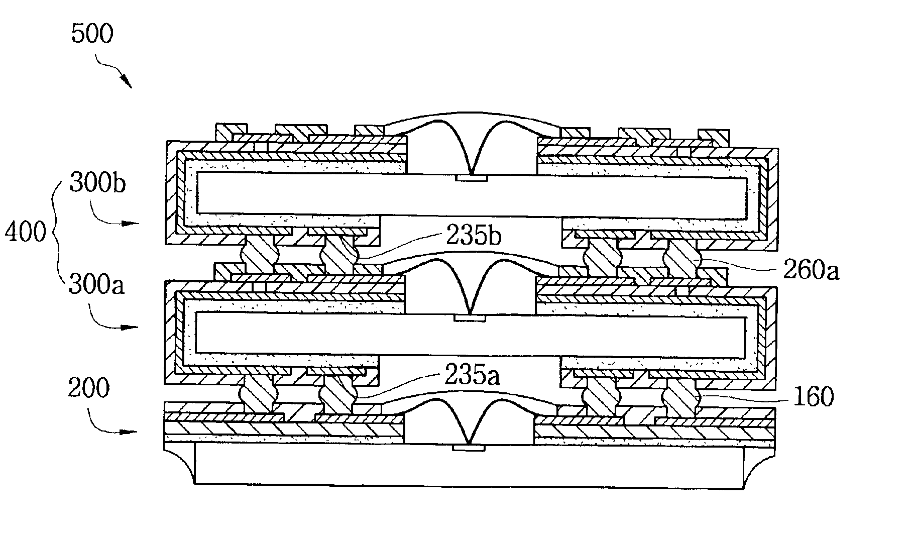
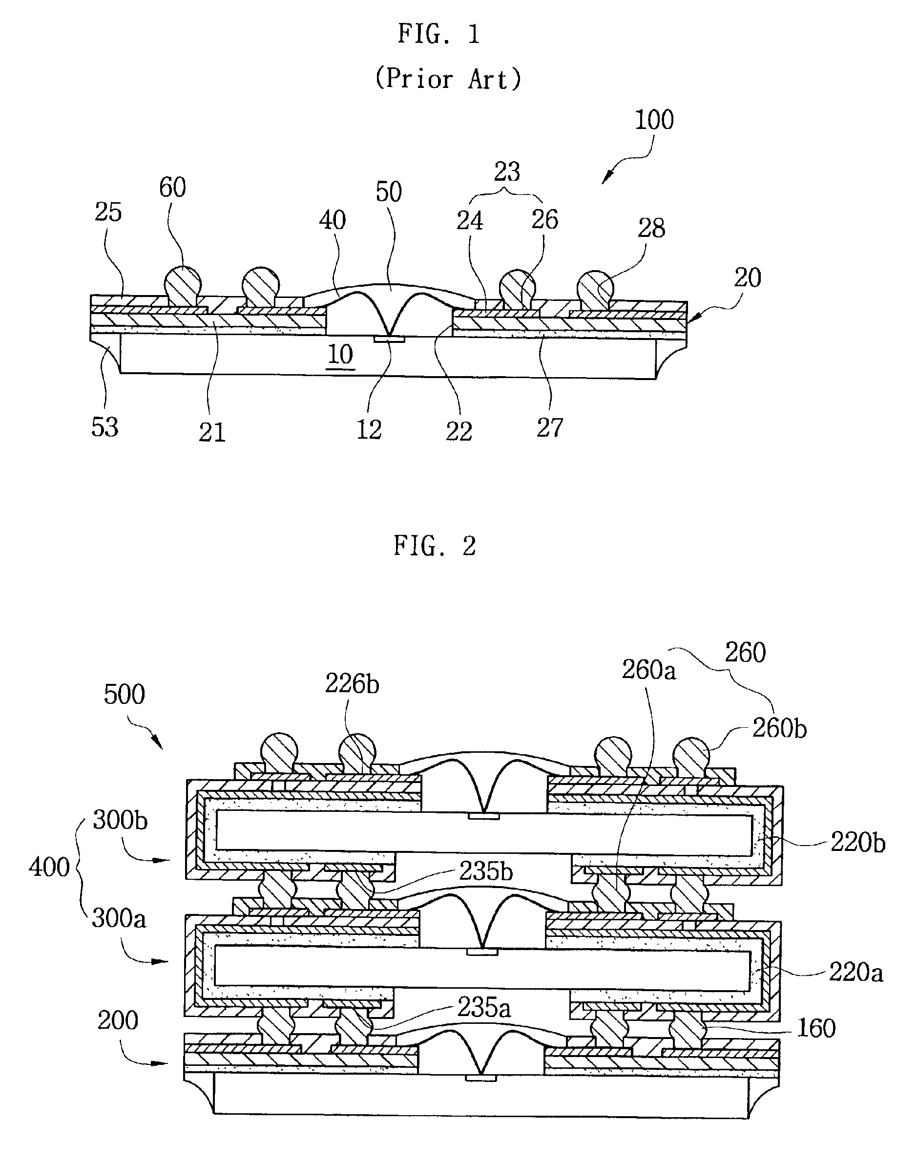
FIG. 2 is a cross-sectional view of a stack package 500 using a flexible double wiring substrates 220a and 220b in accordance with an embodiment of the present invention. With reference to FIG. 2, stack package 500 has a stack structure by three-dimensionally stacking stacked unit package 400 embodied by the present invention on the CSP 100 of FIG. 1. (CSP 100 is hereinafter referred to as “base package 200”.) Stacked unit package 400 consists of a plurality of single unit packages 300, such as, a first unit package 300a and a second unit package 300b. First unit package 300a comprises a bottom surface attached to connection terminals 160 of base package 200 and a top surface with first connection terminals 260a electrically connected to connection terminals 160 of base package 200. Second unit package 300b comprises a bottom surface attached to first connection termina...


PUM


Abstract

A Chip Scale Package (CSP) type unit package including a semiconductor chip and a double wiring substrate, the double wiring substrate including an adhesive and a flexible tape having an upper surface with a first wiring pattern, a lower surface with a second wiring pattern and a plurality of vias electrically connecting portions of the first and second wiring patterns. Additionally, the unit package may be stacked on a conventional base package or on another unit package, where stacked packages are electrically interconnected.

Description

BACKGROUND OF THE INVENTION1. Field of the InventionThe present invention relates to semiconductor packaging technology, and more particularly to a stack package using a flexible double wiring substrate.2. Description of the Related ArtIt has been long desired to provide low-cost semiconductor chip packages that are lighter, smaller, faster and multi-functional, having improved reliability. In order to satisfy this goal, a package assembly technique has been developed, utilizing a recently introduced Ball Grid Array (BGA) package. Compared to the conventional plastic package, the BGA package reduces the mounting area on a motherboard and has improved electrical properties.The BGA package uses a printed circuit board instead of a conventional plastic package lead frame. The surface of the printed circuit board that is opposite to the surface with a semiconductor chip attached thereto, contains an area for forming solder balls. Thus, the BGA package improves the mounting density on th...

Claims


Application Information

Patent Timeline
Patent Type & Authority Patents(United States)
IPC IPC(8): H01L23/02H01L23/14H01L23/12H01L23/48H01L23/34H01L29/40H01L23/31H01L23/498H01L25/10
CPCH01L23/3114H01L23/4985H01L25/105H01L2224/73215H01L2224/32225H01L2225/1058H01L2225/1041H01L2225/1023H01L24/48H01L2924/15311H01L2924/01079H01L2224/4824H01L2924/01078H01L2924/00H01L2224/05599H01L2224/45099H01L2224/85399H01L2924/00014H01L2924/181H01L2924/00012H01L2224/45015H01L2924/207H01L23/14
Inventor KIM, SHIN
Owner SAMSUNG ELECTRONICS CO LTD
Why Eureka
Try Eureka