Method of inter-field critical dimension control

a critical dimension control and inter-field technology, applied in the direction of semiconductor/solid-state device testing/measurement, instruments, photomechanical equipment, etc., can solve the problems of reducing the stability of semiconductor chips obtained by dies, differences among manufacturing devices, and affecting the critical dimension control in the wafer manufacturing process. , to achieve the effect of simple and effectiv

Inactive Publication Date: 2005-04-05
TAIWAN SEMICON MFG CO LTD
View PDF4 Cites 3 Cited by
  • Summary
  • Abstract
  • Description
  • Claims
  • Application Information

AI Technical Summary

Benefits of technology

In view of this, the present invention relates to a method of inter-field critical dimension control for a wafer with a plurality of dies manufactured by exposure. The exposure energy of exposure is calibrated to compensate for the inter-field critical dimension difference due to the whole wafer manufacturing process. Thus, there is no need to determine a critical individual process in the wafer manufacturing process, and the inter-field critical dimension control is effective and simplified.

Problems solved by technology

This reduces the stability of the semiconductor chips obtained by the dies 10.
It is obvious that a difference exists among manufacturing devices for each of the individual process and the difference may affect the critical dimension control in the wafer manufacturing process.
Further, it is difficult to find a critical process for wafer manufacture since each of the individual process may use different manufacturing devices.
Consequently, it is not possible to improve the inter-field critical dimension by calibration of any individual process.

Method used


Image

  • Method of inter-field critical dimension control
  • Method of inter-field critical dimension control
  • Method of inter-field critical dimension control

Examples


Embodiment Construction

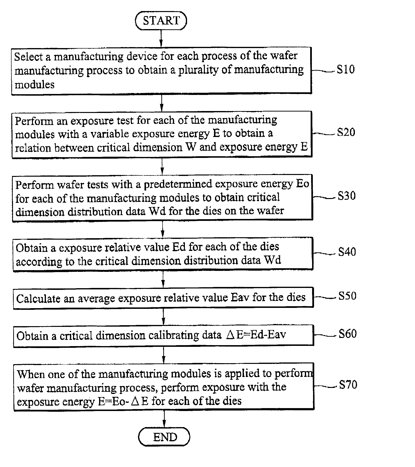
The method of inter-field critical dimension control of the present invention can be hereinafter described with reference to FIG. 3. The method of inter-field critical dimension control of the present invention is applied to a wafer with a plurality of dies. The wafer manufacturing process has an exposure process.

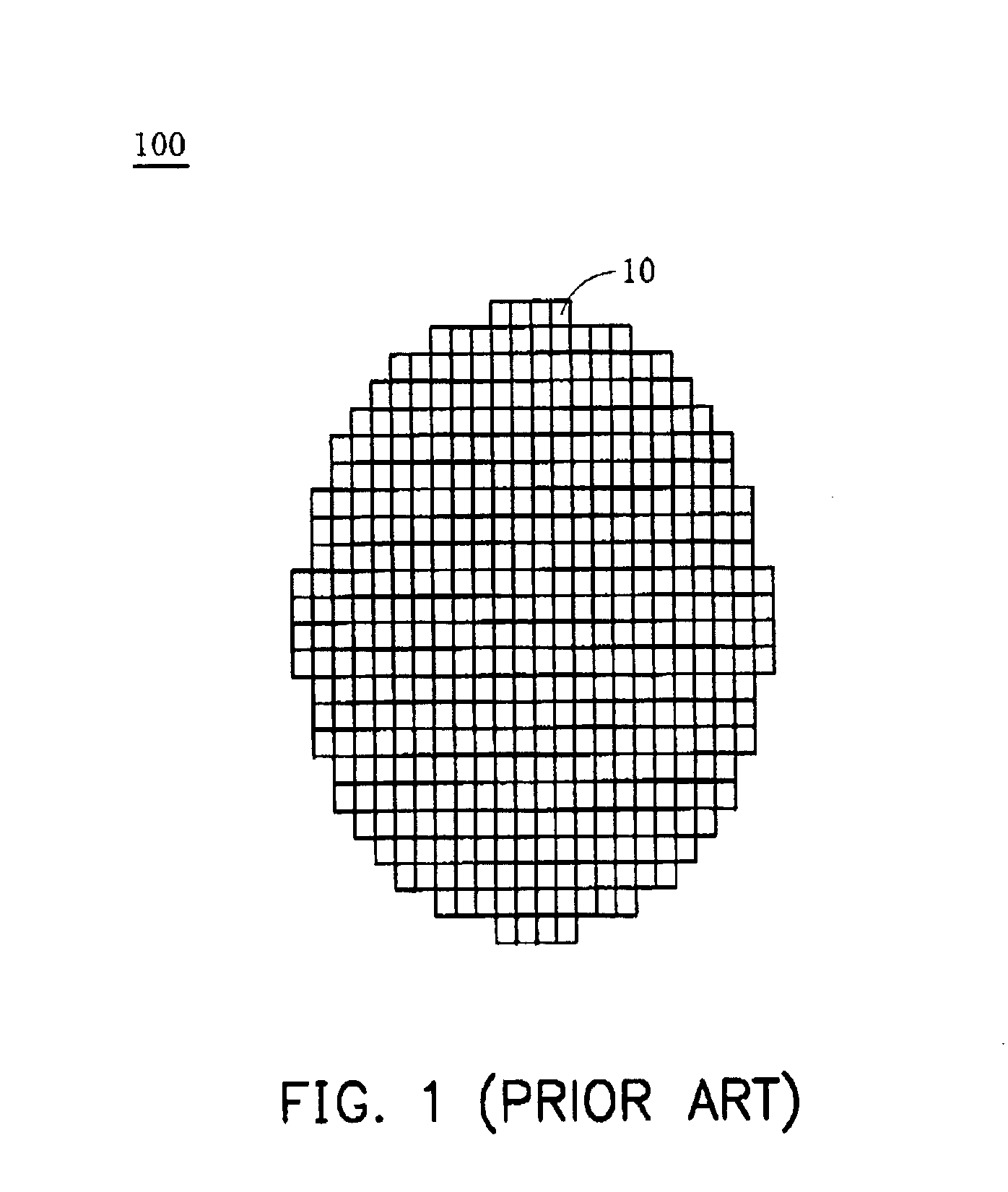
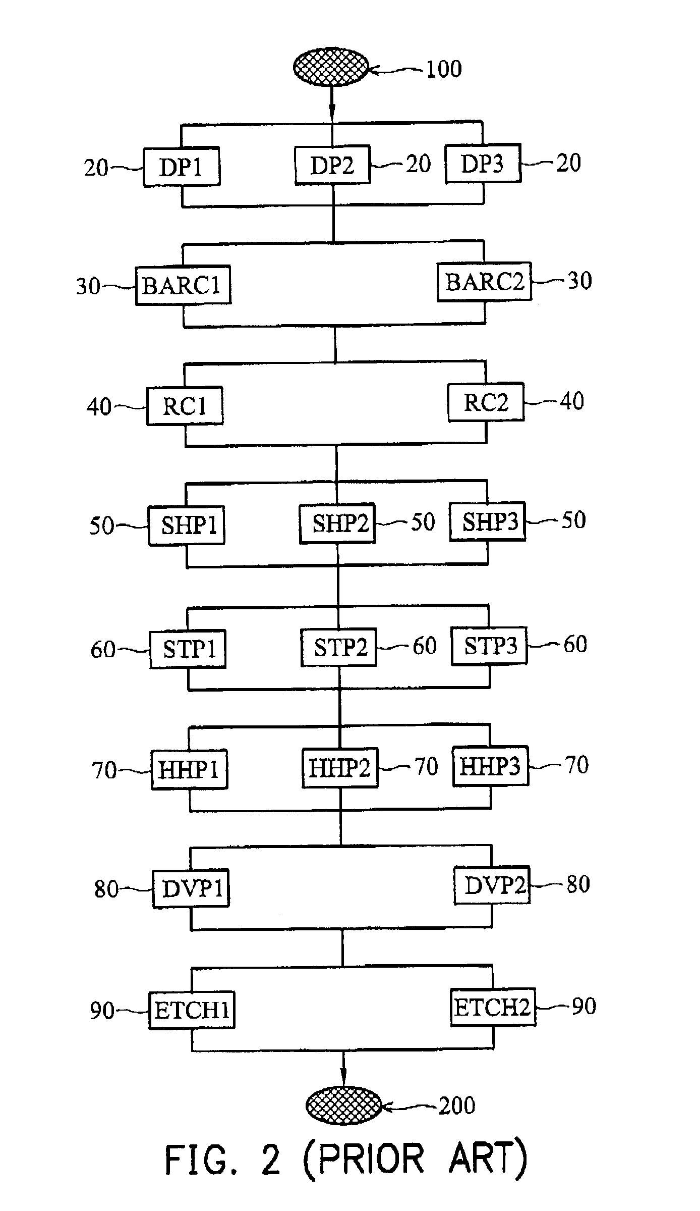
First, before an experiment for the wafer manufacturing process begins, it is necessary to select a manufacturing device for each process of the wafer manufacturing process to obtain a plurality of manufacturing modules (step S10), such as the 1296 manufacturing modules in FIG. 2. It should be noted that in practical industrial application, not all of the 1296 manufacturing modules are generally applied in the wafer manufacturing process. In some cases, it is possible that only one of the manufacturing modules, such as a manufacturing module shown as DP1-BARC1-RC1-SHP1-STP1-HHP1-DVP1-ETCH1 in FIG. 2, is applied to perform all the wafer manufacturing process. Consequently, t...


PUM

PropertyMeasurementUnit
dimensionaaaaaaaaaa
critical dimension distributionaaaaaaaaaa
critical dimensionaaaaaaaaaa

Abstract

A method of inter-field critical dimension control. The method is applied to a wafer with a plurality of dies manufactured by a wafer manufacturing process that includes exposure. According to the method, a plurality of manufacturing modules is obtained by selecting a manufacturing device for each process of the manufacture. Then, for each manufacturing module, exposure is performed with a predetermined exposure energy to obtain critical dimension distribution data corresponding to the predetermined exposure energy, and critical dimension calibration data for each of the dies is further determined. Thus, when one of the manufacturing modules is applied to perform the manufacture, an exposure energy for each of the dies is determined according to the predetermined exposure energy and the critical dimension calibration data for each of the dies, and the manufacture is performed with the exposure energy on each of the dies for the manufacturing module.

Description

BACKGROUND OF THE INVENTION1. Field of the InventionThe present invention relates to a method of critical dimension control, and particularly to a method of inter-field critical dimension control for a wafer in semiconductor technique.2. Description of the Related ArtA critical dimension (CD) of a circuit is commonly defined as the smallest width of a line or the smallest space between two lines. Generally, the critical dimension is an important factor for the wafer manufacturing process. FIG. 1 shows a scheme of a wafer 100, which has a plurality of dies (or fields) 10. Generally, control of the critical dimension of the wafer 100 includes intra-field CD control and inter-field (or die-to-die) CD control. The intra-field CD control refers to control of the critical dimension in a individual die 10, so that the line width in the individual die 10 has approximately the same value. Meanwhile, the inter-field CD control refers to control of the critical dimension between the dies 10, s...

Claims


Application Information

Patent Timeline
Patent Type & Authority Patents(United States)
IPC IPC(8): G03F7/20G03F7/16G03F7/40G03F9/00
CPCG03F7/70625
Inventor GAU, TSAI-SHENGYEN, ANTHONYLIN, BURN J.
Owner TAIWAN SEMICON MFG CO LTD
Why Eureka
Try Eureka