Phase-change memory devices with a self-heater structure

a memory device and self-heating technology, applied in the direction of digital storage, semiconductor/solid-state device details, digital storage, etc., can solve the problems of joule heating, affecting reliability, and affecting reliability,

Active Publication Date: 2005-05-17
SAMSUNG ELECTRONICS CO LTD
View PDF3 Cites 386 Cited by
  • Summary
  • Abstract
  • Description
  • Claims
  • Application Information

AI Technical Summary

Benefits of technology

[0008]In additional embodiments of the present invention, the first electrode is at a first level with respect to the substrate and the second electrode is at a second level with respect to the substrate. The first level and the second level are different distances from the substrate. The phase-change memory layer may be at a third level with respect to the substrate where the third level is a distance from the substrate that is greater than a distance from the substrate of the first level and less than a distance from the substrate of the second level. A third electrode may also be provided at a fourth level with respect to the substrate. The fourth level may be a distance from the substrate that is less than the distance from the substrate of the third level. The third electrode may electrically connect the second electrode to the phase-change memory layer.

Problems solved by technology

In this structure, the contact area between the phase-change material layer and the lower electrode is reduced as much as possible so that the current density of the two contact surfaces is rapidly increased, thus causing Joule heating.
However, area variations within a permitted range, typically, cannot be easily obtained because of current photolithographic and etching restrictions.
However, since the contact area between the phase-change material layer and the lower electrode is small, the contact resistances may vary within a large range, thus degrading reliability.

Method used


Image

  • Phase-change memory devices with a self-heater structure
  • Phase-change memory devices with a self-heater structure
  • Phase-change memory devices with a self-heater structure

Examples


Embodiment Construction

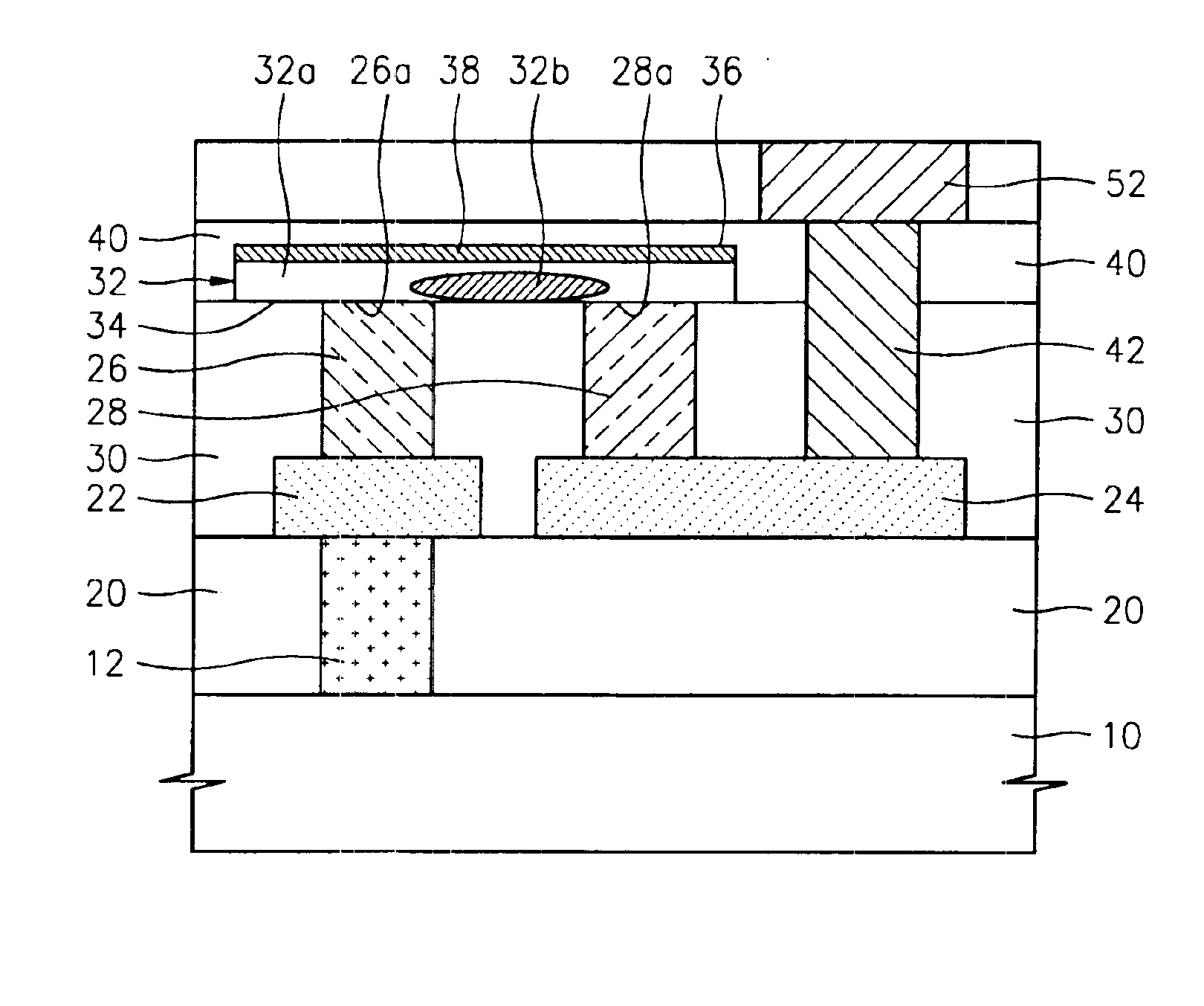
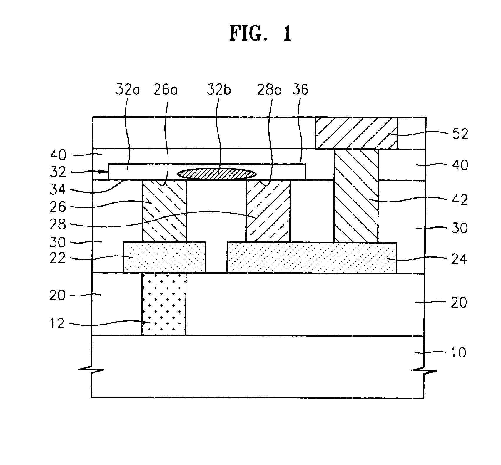
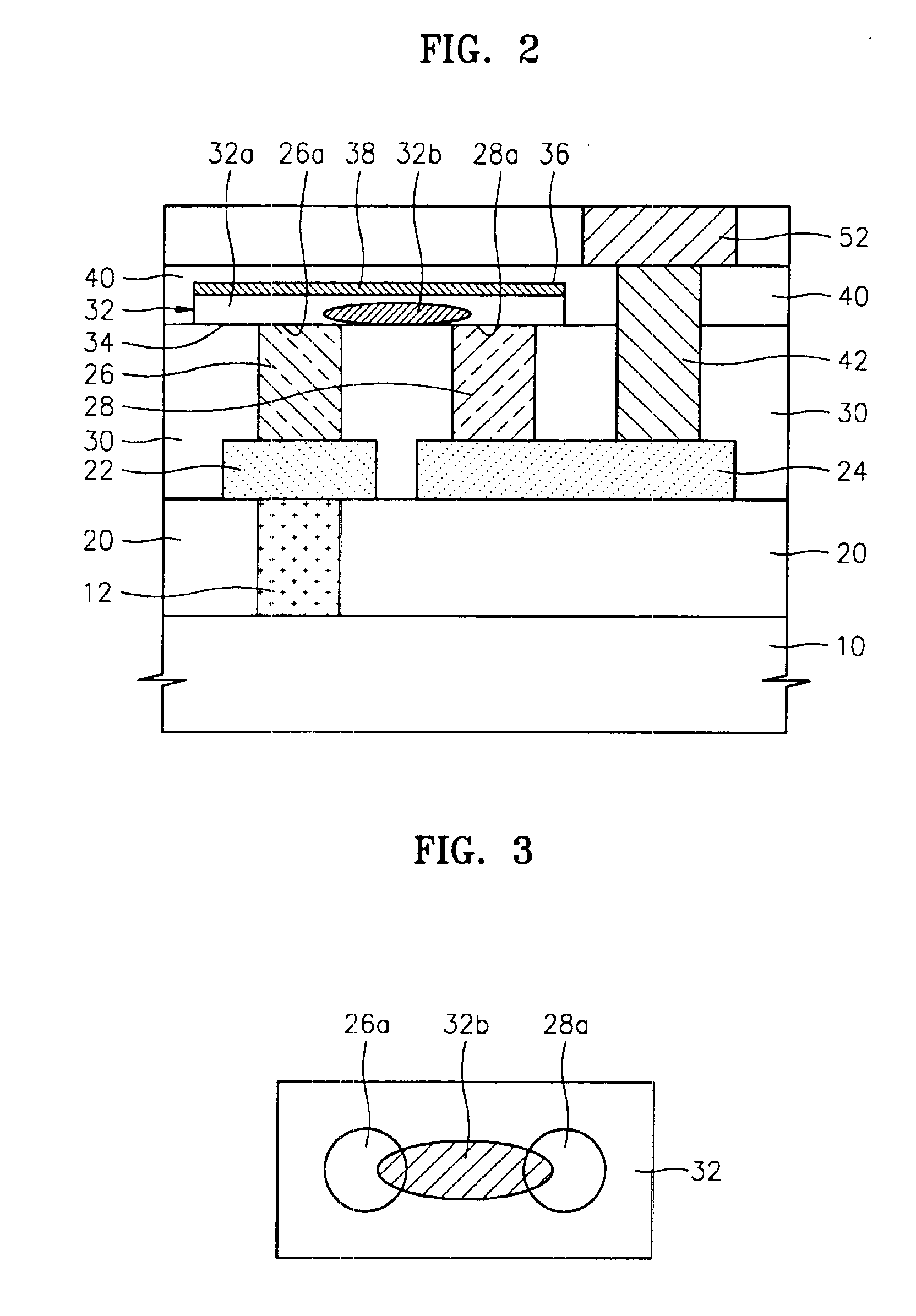
[0026]The present invention will now be described more fully with reference to the accompanying drawings, in which preferred embodiments of the invention are shown. This invention may, however, be embodied in different forms and should not be construed as being limited to the embodiments set forth herein. Rather, these embodiments are provided so that this disclosure will be thorough and complete, and will fully convey the scope of the invention to those skilled in the art. In the drawings, the size or thickness of layers and regions are exaggerated for clarity. Like numbers refer to like elements. As used herein the term “and / or” includes any and all combinations of one or more of the associated listed items.

[0027]It will be understood that although the terms first and second may be used herein to describe various regions, layers, and / or sections, these regions, layers, and / or sections should not be limited by these terms. These terms are only used to distinguish one region, layer,...


PUM


Abstract

Phase change memory devices include a phase-change memory layer on a semiconductor substrate. The phase-change memory layer has a major axis that is substantially parallel to a major axis of the semiconductor substrate and has a first surface and a second surface opposite the first surface that are substantially parallel to the major axis of the phase-change memory layer. A first electrode is provided on the semiconductor substrate that is electrically connected to the first surface of the phase-change memory layer in a first contact region of the phase-change memory layer. A second electrode is provided on the semiconductor substrate that is electrically connected to the phase-change memory layer in a second contact region of the phase-change memory layer. The second contact region is space apart from the first contact region.

Description

CLAIM OF PRIORITY[0001]This application claims priority from Korean Patent Application No. 2003-11356, filed on Feb. 24, 2003, in the Korean Intellectual Property Office, the contents of which are incorporated herein by reference in its entirety.FIELD OF THE INVENTION[0002]The present invention relates to phase-change memory devices, and more particularly, to phase-change random access memory (PRAM) using characteristics of chalcogenide.BACKGROUND OF THE INVENTION[0003]Conventional PRAMs are memory devices using characteristics of a phase-change material, such as chalcogenide, the electric resistance of which varies according to its crystalline phase. A phase-change material layer formed of chalcogenide is partially changed to be in a crystalline or amorphous phase according to the applied current profile. The crystalline phase of a phase-change material layer can be selectively changed by, for example, temperature variation. That is, a temperature variation occurs by adjusting the ...

Claims


Application Information

Patent Timeline
Patent Type & Authority Patents(United States)
IPC IPC(8): H01L45/00H01L27/10
CPCH01L45/06H01L45/144H01L45/126H01L45/1226H01L27/2436H10B63/30H10N70/823H10N70/8413H10N70/231H10N70/8828H01L27/10
Inventor YI, JI-HYEHIDEKI, HORIIHA, YONG-HO
Owner SAMSUNG ELECTRONICS CO LTD
Why Eureka
Try Eureka