Slim USB male connector with system grounding

Inactive Publication Date: 2005-05-24
MEGAFORCE
4 Cites 21 Cited by

AI-Extracted Technical Summary

Problems solved by technology

When inserting the USB connector 90 into a stacked USB socket, it...

Method used

[0030]Reference is made to FIG. 3 and FIG. 3A, which are perspective views of the slim USB male connector applied in a storage device from different views. The slim USB male connector 2 can be applied in different electrical devices with advantages of compact and convenient carrying. The slim USB male connector with system grounding 2 further comprises a storage device 3 extending from an end of the circuit board 10 and formi...

Abstract

A slim USB male connector with system grounding mates with a USB socket. The USB male connector is received in a space between a mating board and a bottom wall of a frame of the USB socket. The USB male connector has a circuit board formed with a plurality of circuits on top and bottom surfaces thereof. Four contacts are formed on the top surface of the circuit board and connected with the circuits thereon. A grounding plate is mounted on the bottom surface of the circuit board and connected with a grounding circuit on the circuit board. The grounding plate connects to the tongues of the USB socket to ground the system.

Application Domain

Coupling protective earth/shielding arrangementsConnection contact member material

Technology Topic

USBGround plate

Image

  • Slim USB male connector with system grounding
  • Slim USB male connector with system grounding
  • Slim USB male connector with system grounding

Examples

  • Experimental program(1)

Example

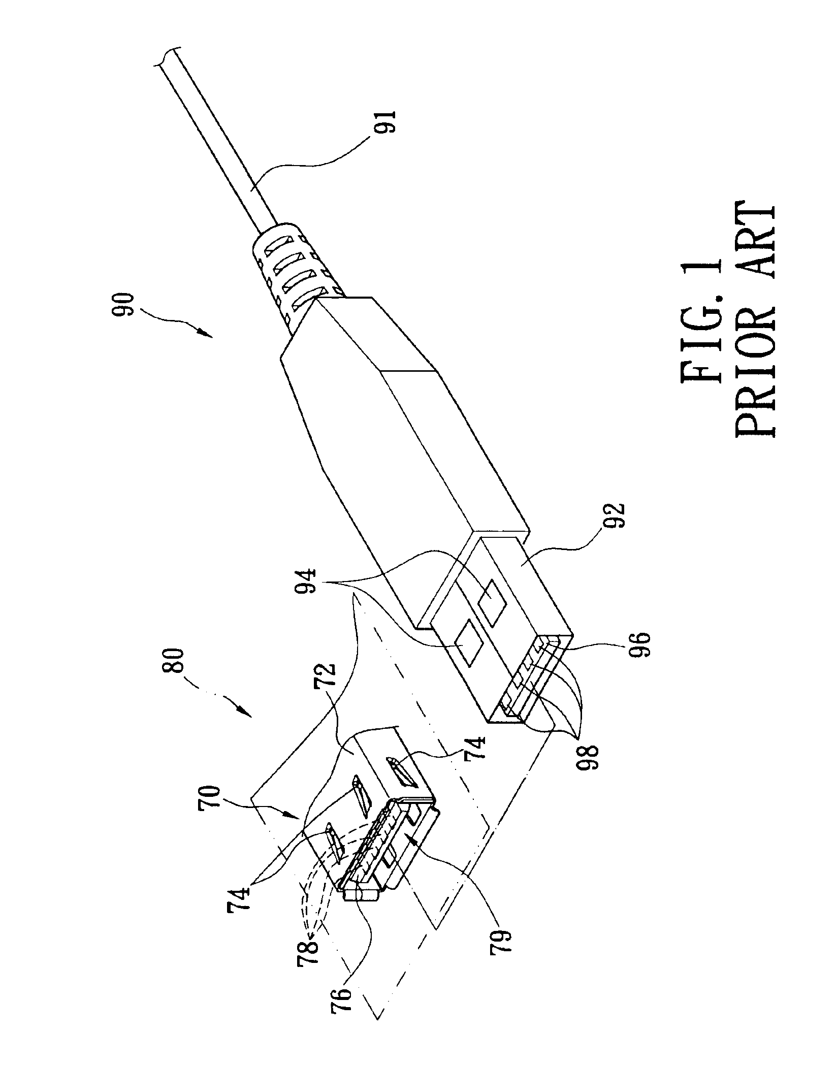
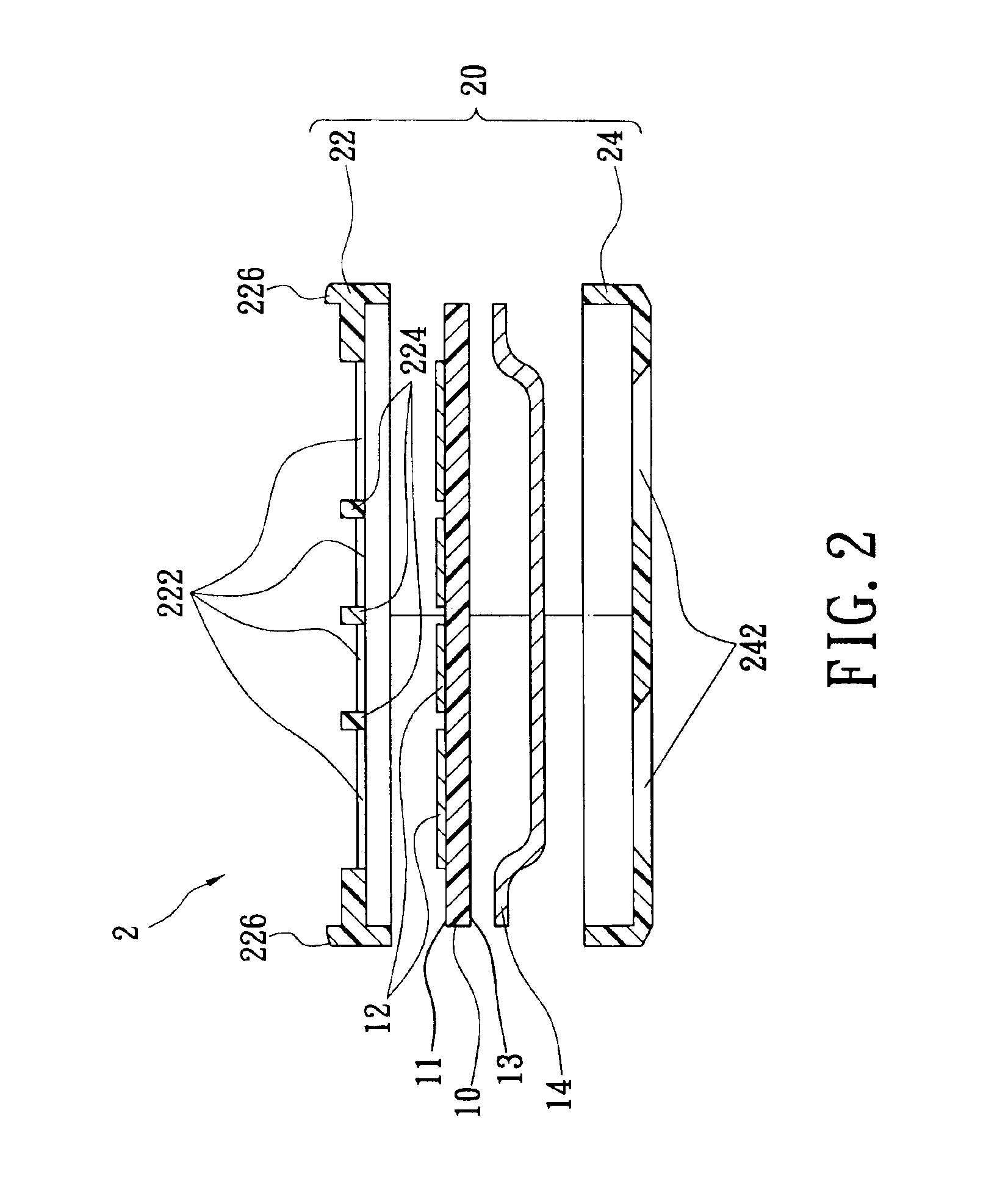
[0023]Reference is made to FIG. 2, which is an exploded cross-sectional view of a slim USB male connector with system grounding according to the present invention. The slim USB male connector 2 is mated with the USB socket 70 of the prior art. The USB socket 70 as mentioned above, has a frame 72 stamped with a plurality of elastic tongues 74, a mating board 76 mounted in the frame 72, and four terminals 76 mounted on a bottom of the mating board 76. A space 79 is formed between the mating board 76 and a bottom wall of the frame 72.
[0024]The USB male connector 2 is received in the space 79 of the USB socket 70. The USB male connector 2 comprises a circuit board 10, four contacts 12, and a grounding board 14.
[0025]The circuit board 10 is formed with a plurality of circuits (not shown) on a top surface 11 and a bottom surface 13 thereof.
[0026]The four contacts 12 are made of conductive metal, and mounted on the top surface 11 of the circuit board 10 and connected with the corresponding circuits thereon. The size of the four contacts 12 complies with the four contacts 78 of the USB socket 70, both physically and electrically. The four contacts 12 are contiguously in contact with the contacts 78 of the USB socket 70.
[0027]The grounding plate 14 is formed by stamping a metal board. The grounding plate 14 has two ends respectively soldered on the bottom 13 of the circuit board 10 and connected with a grounding circuit thereon. The grounding plate 14 is connected to the tongues 74 of the USB socket 70 for achieving system grounding.
[0028]An insulative housing 20 covers a periphery of the circuit board 10. The insulative housing 20 has an upper housing 22 and a lower housing 24 respectively formed with grooves 222, 242 for exposing the contacts 12 and the grounding plate 14 outside. The upper housing 22 has four upper grooves 222, and protruding walls 224, 226 respectively protruding from two side edges thereof and between the upper grooves 22. The protruding walls 226 are respectively inserted into side gaps between the mating board 76 and two sides of the frame 72 of the USB socket 70.
[0029]The lower housing 24 of the insulative housing 20 has a pair of grounding grooves 242 for exposing the grounding plate 14 outside and receiving the tongues 74 of the frame 72 of the USB socket 70 therein. The grounding plate 14 is electrically connected to the tongues 74 with a fixing function.
[0030]Reference is made to FIG. 3 and FIG. 3A, which are perspective views of the slim USB male connector applied in a storage device from different views. The slim USB male connector 2 can be applied in different electrical devices with advantages of compact and convenient carrying. The slim USB male connector with system grounding 2 further comprises a storage device 3 extending from an end of the circuit board 10 and forming a flash memory card 1. The flash memory card 1 is more compact and slimmer due to the slim USB male connector 2. A plugging portion of the flash memory card 1 is as thin as the storage device 3, which is beneficial when applied in an electrical device such as, for example, a PDA, digital camera or notebook. A circuit layout of the storage device 3 is not the character of the present invention, and so is not mentioned here.
[0031]Referring to FIG. 4 and FIG. 5, FIG. 4 is a top view of a flash memory card with the present invention plugged in an USB socket, and FIG. 5 is a cross-sectional view along line 5—5 in the FIG. 4. A particularly distinguishing feature of the slim male connector 2 of the present invention is that the slim male connector 2 abandons the frame of prior art and replaces the same with an insulative housing 20 of non-metal material. The contacts 12 and the grounding plate 14 are hidden in the insulative housing 20. The slim male connector 2 is only inserted in the lower space 79 of the USB socket 70. The slim male connector 2 entirely complies with the specifications and functions of USB and has a hidden grounding design for system grounding. The total height of the slim male connector 2 of the present invention is about half of the USB connector of the prior art, and the width thereof is reduced as well. The advantages of compact of the present invention are especially manifest when applied in the flash memory.
[0032]Reference is made to FIG. 6, which is a side view of the slim USB male connector applied in computer peripheral device. The slim male connector 2 of the present invention further comprises a cable 3′ connecting with an end of the circuit board 10 and electrically connecting with the circuits of the circuit board 10. The cable 3′ can be connected with a computer peripheral 4 such as, for example, a mouse or keyboard. Conversely, the cable 3′ can be connected with an electrical connector 4′ and form a connecting cable (as shown in FIG. 7) for transferring data between electric devices.
[0033]It is to be understood, however, that even though numerous characteristics and advantages of the present invention have been set forth in the foregoing description, together with details of the structure and function of the invention, the disclosure is illustrate only, and changes may be made in detail, especially in matters of shape, size, and arrangement of parts within the principles of the invention to the full extent indicated by the broad general meaning of the terms in which the appended claims are expressed.

PUM

no PUM

Description & Claims & Application Information

We can also present the details of the Description, Claims and Application information to help users get a comprehensive understanding of the technical details of the patent, such as background art, summary of invention, brief description of drawings, description of embodiments, and other original content. On the other hand, users can also determine the specific scope of protection of the technology through the list of claims; as well as understand the changes in the life cycle of the technology with the presentation of the patent timeline. Login to view more.
Why Eureka
Try Eureka