Method and system for measuring stray light
a technology of exposure apparatus and stray light, which is applied in the direction of optical radiation measurement, photomechanical apparatus, instruments, etc., can solve the problems of significant influence on the accuracy and reliability of measured data, time-consuming process of obtaining measurement data, and significant influence on the performance of semiconductor devices. achieve the effect of fast and effective stray light measuremen
- Summary
- Abstract
- Description
- Claims
- Application Information
AI Technical Summary
Benefits of technology
Problems solved by technology
Method used
Image
Examples
first embodiment
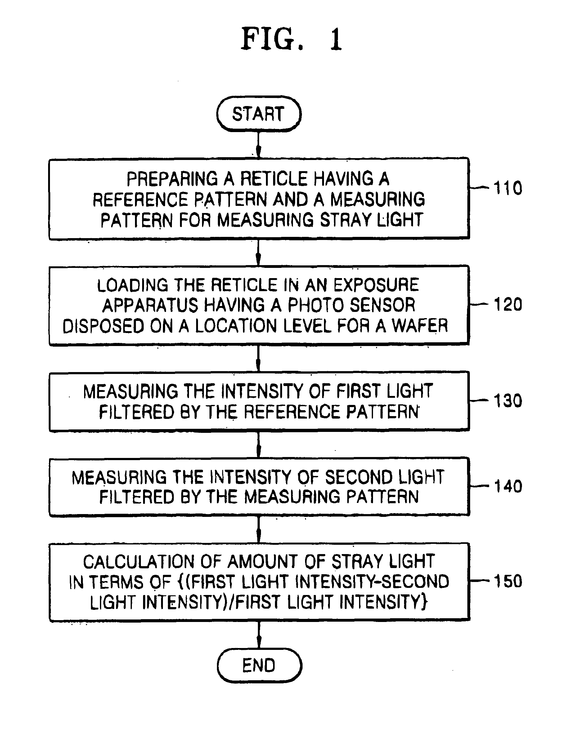
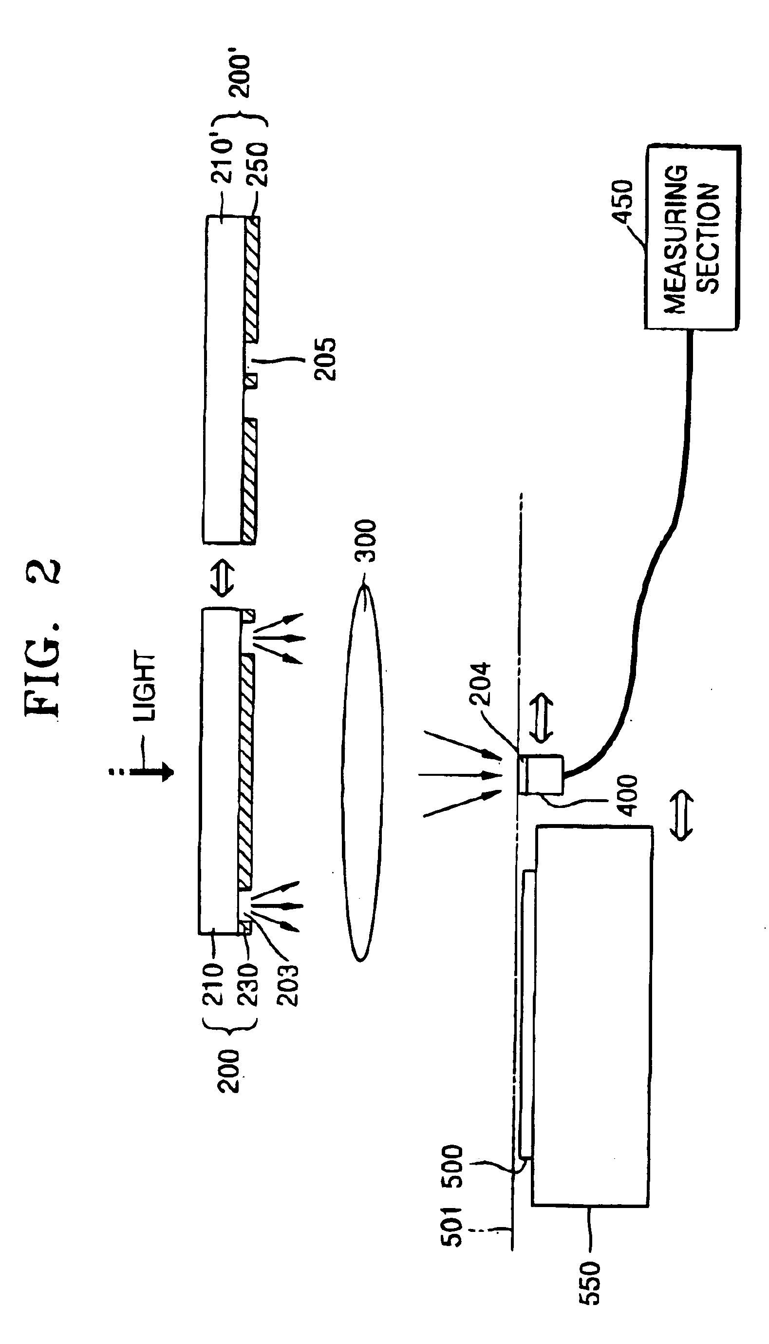
[0037]Therefore, in the present invention, the size (or width) of the photo sensing region is relatively large, i.e., larger than needed to measure stray light, so that it can be used not only for measuring stray light, but also for focusing and aligning a wafer. That is, the width of a sensing region 204 of the image sensor 400 may be a few tens of microns, e.g., a length of a side of the square is a few tens microns with respect to the size of the reticle.
[0038]If the size of the photo sensing region 204 is a few tens of microns, the intensity data of the sensed stray light within a range of a few microns, more specifically, about 1˜20 μm, and, more practically, up to about 10 μm, cannot be used for evaluating an effect of stray light. In order to solve this problem, a measuring pattern system as depicted in FIGS. 3A and 3B is introduced in accordance with the first embodiment of the present invention.
[0039]Referring to FIGS. 2, 3A, and 3B, the measuring pattern system includes pa...
second embodiment
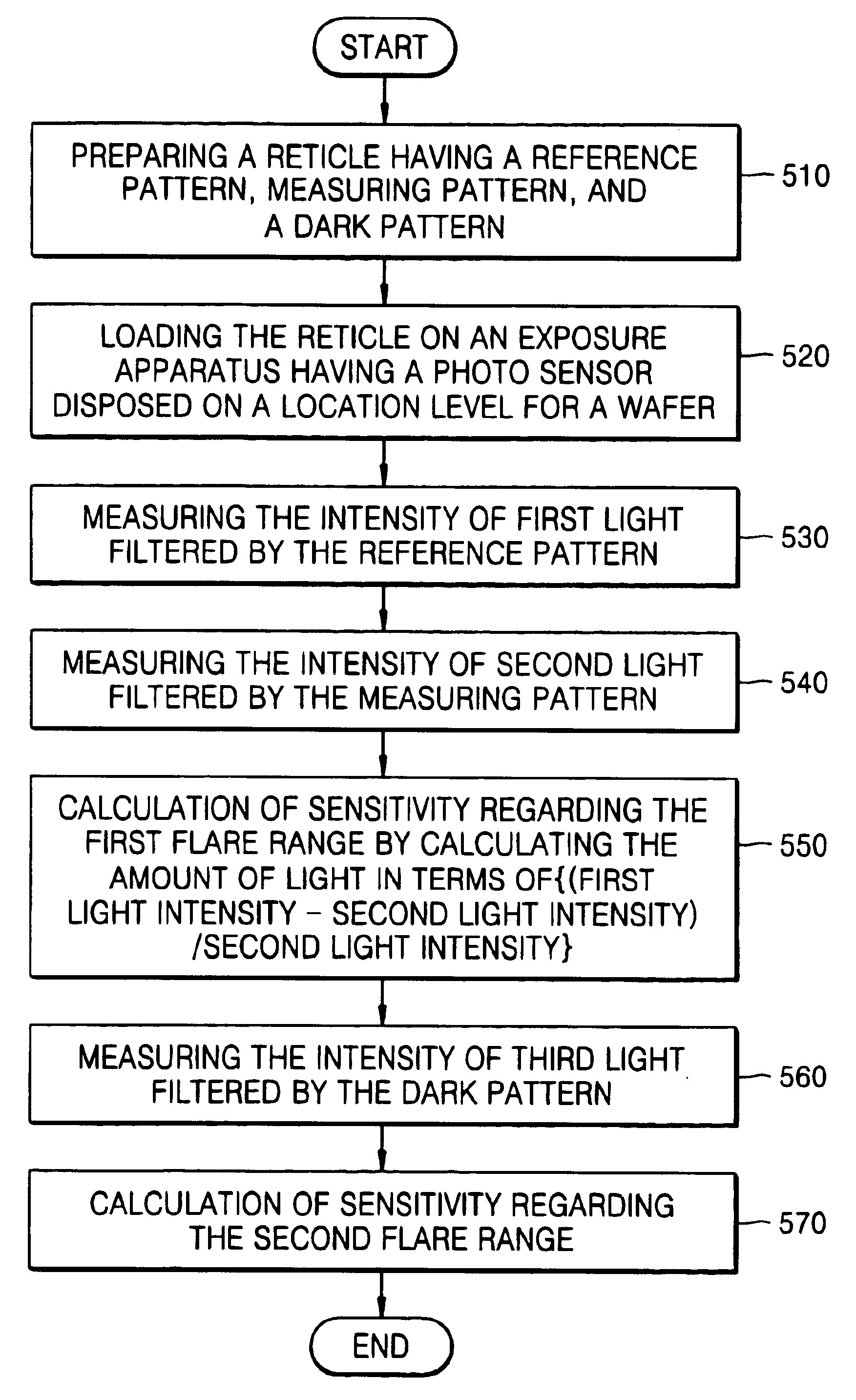
[0063]Referring to FIGS. 5 and 6, a stray light measuring pattern system having an opaque pattern 270 is formed on a transparent substrate 210 of a reticle 200, in step 510. In the second embodiment, the measuring pattern system includes the opaque pattern 270 in addition to the measuring pattern 230 and the reference pattern 250 as described with reference to FIGS. 3A and 3B. The opaque pattern 270 can be formed on the same transparent substrate 210 of the reticle 200 as the measuring pattern 230 and the reference pattern 250, or can be formed on a separate transparent substrate.
[0064]The opaque pattern 270 is surrounded by a third open or transparent region 207. The third open region 207 is a light transmitting region, while the opaque pattern 270 is a light shielding or blocking region. The opaque pattern 270 may be sufficiently large to cover the photo sensing region 204 when the opaque pattern 270 is positioned over the sensor 400.
[0065]Using the opaque pattern 270, stray light...
PUM
| Property | Measurement | Unit |
|---|---|---|
| size | aaaaa | aaaaa |
| size | aaaaa | aaaaa |
| size | aaaaa | aaaaa |
Abstract
Description
Claims
Application Information


