Optical sensing device

a technology of optical sensing and optical sensors, which is applied in the field of optical sensing devices, can solve the problems of time-consuming and complicated device structure, and achieve the effects of rapid detection of incident light two-dimensional positions, high accuracy, and rapid detection of information concerning light emitted

Inactive Publication Date: 2006-07-27
HAMAMATSU PHOTONICS KK
View PDF3 Cites 7 Cited by
  • Summary
  • Abstract
  • Description
  • Claims
  • Application Information

AI Technical Summary

Benefits of technology

[0011] In the photodetector in accordance with this aspect of the present invention, light incident on one pixel is detected by a plurality of photosensitive portions constituting the pixel, whereby the photosensitive portions output respective electric currents corresponding to light intensities. Since one set of photosensitive portions are electrically connected to each other in a plurality of pixels arranged in the first direction in the two-dimensional arrangement, the electric current from one photosensitive portion is transmitted to the first direction. Since the other set of photosensitive portions are electrically connected to each other in a plurality of pixels arranged in the second direction in the two-dimensional arrangement, the electric current from the other photosensitive portion is transmitted to the second direction. Thus, the electric current from one photosensitive portion is transmitted to the first direction, whereas the electric current from the other photosensitive portion is transmitted to the second direction, whereby respective luminous profiles in the first and second directions can be obtained independently from each other. As a result, a quite simple configuration of arranging a plurality of photosensitive portions in one pixel can rapidly detect a two-dimensional position of incident light.
[0012] In this aspect of the present invention, the range from the minimum value detected by the first minimum value detecting circuit to a value greater than the minimum value by a predetermined value is employed as an A/D conversion range, and the respective voltages outputted from the first integra

Problems solved by technology

In the above-described known art, however, an image memory is required for storing the obtained image data, which causes a complicated structure of the device.
Besides, since tw

Method used


Image

  • Optical sensing device
  • Optical sensing device
  • Optical sensing device

Examples


Embodiment Construction

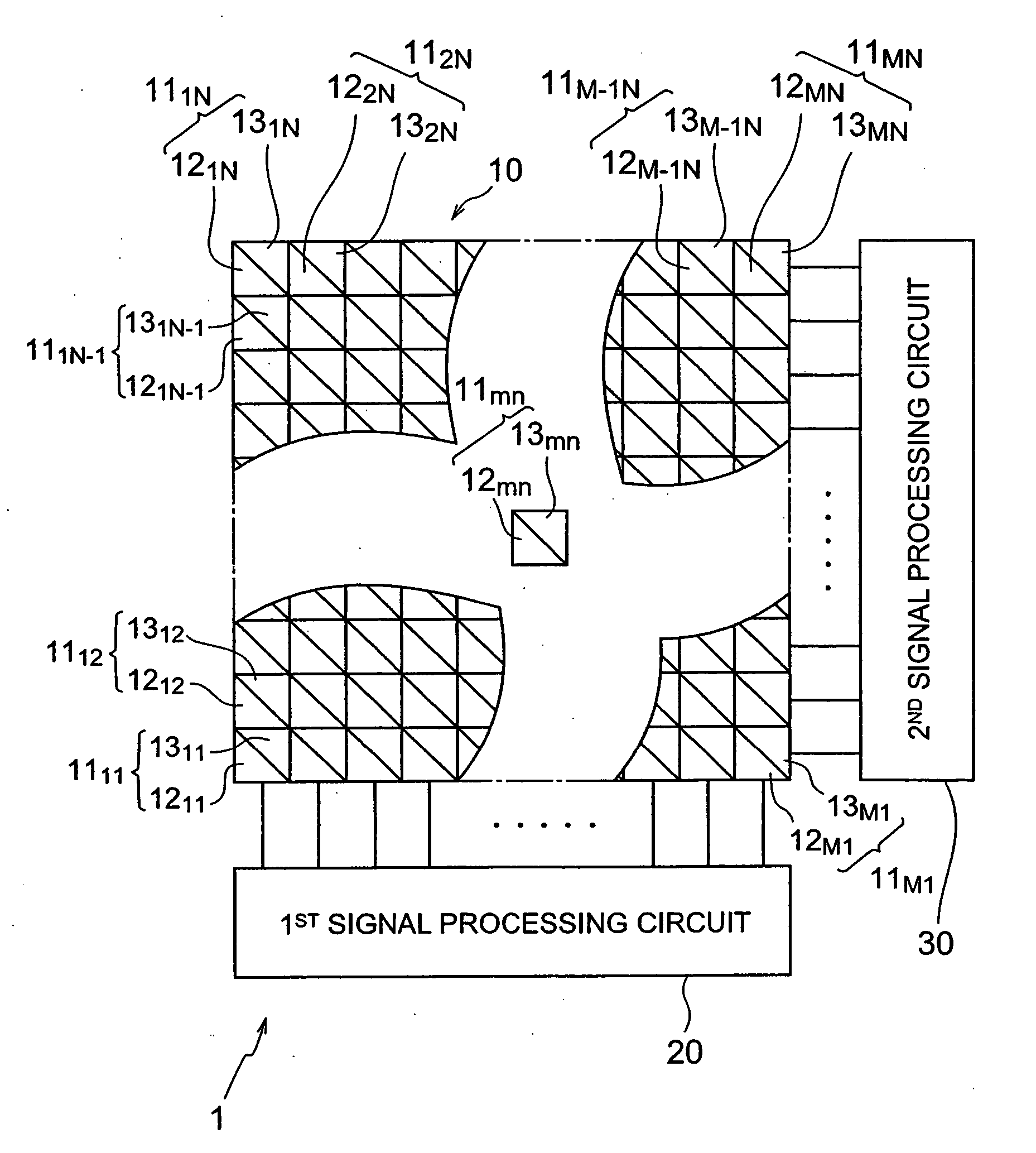
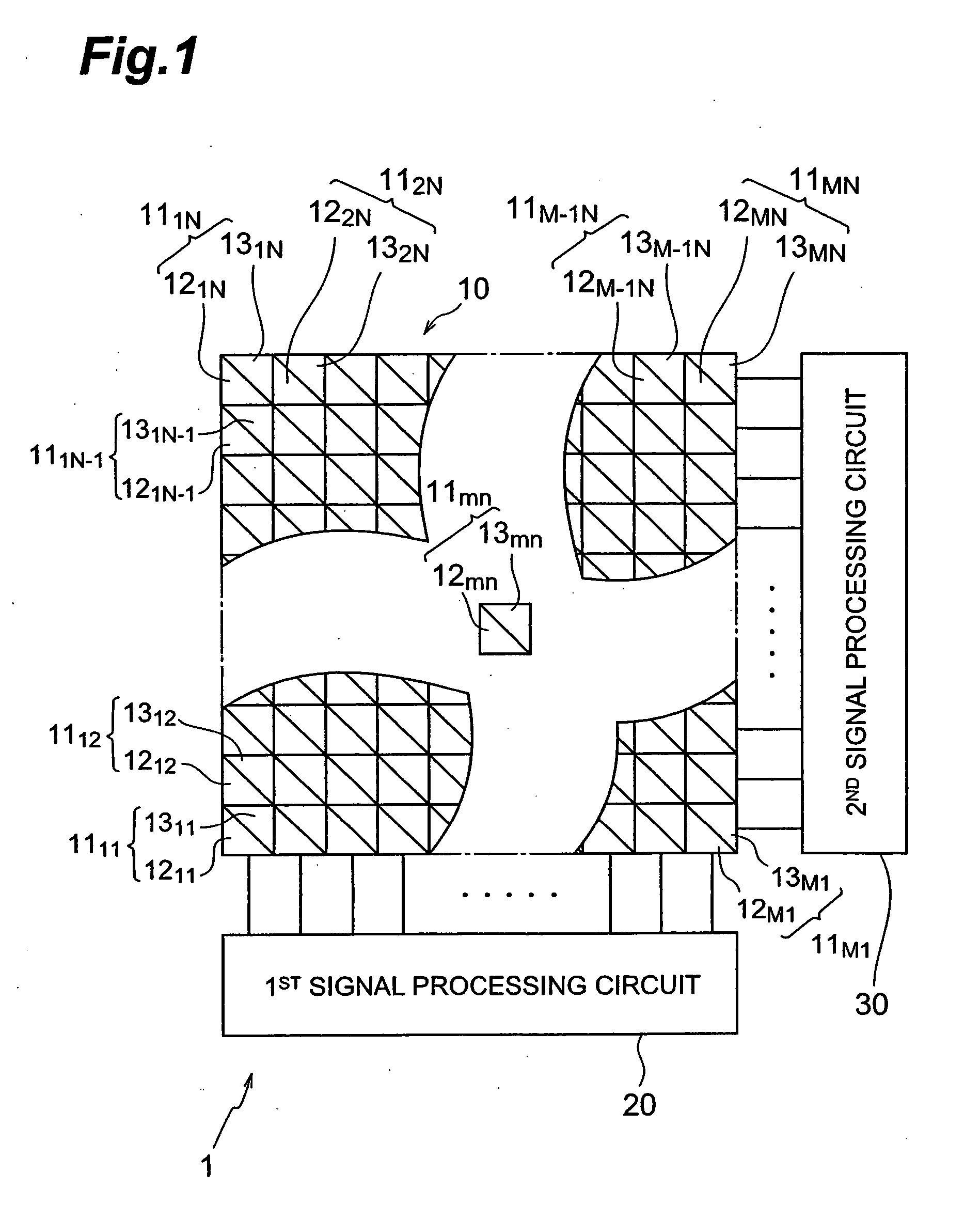
[0056] The photodetector in accordance with an embodiment of the present invention will be explained with reference to the drawings. In the explanation of the drawings, constituents identical to each other or those having functions identical to each other will be referred to with numerals identical to each other without repeating their overlapping explanations. In the following, each of parameters M and N is assumed to be an integer of 2 or greater. Parameter m is assumed to be a given integer of at least 1 but not greater than M whereas parameter n is assumed to be a given integer of at least 1 but not greater than N unless otherwise specified.

[0057]FIG. 1 is a conceptual schematic diagram illustrating the photodetector in accordance with this embodiment. As shown in FIG. 1, the photodetector 1 in accordance with the embodiment includes a photosensitive region 10, a first signal processing circuit 20, and a second signal processing circuit 30. The photodetector 1 detects an incide...


PUM


Abstract

First integrating circuits 110 convert electric currents from one group of photosensitive portions electrically connected to each other in a plurality of pixels arranged in a first direction into voltages, and output the voltages. First S/H circuits 130 hold and output the voltages outputted from the first integrating circuits 110. A first maximum value detecting circuit 140 detects the maximum value of the voltages outputted from the first S/H circuits 130. First level shift circuits 170 shift levels of the voltages outputted from the first S/H circuits 130. A first A/D converter circuit 180 sets a range from the maximum value detected by the first maximum value detecting circuit 140 to a value smaller than the maximum value by a predetermined value as an A/D conversion range, and converts the voltages outputted from the first S/H circuits 130 into digital values within the A/D conversion range.

Description

TECHNICAL FIELD [0001] The present invention relates to a photodetector which detects two-dimensional positions where light is incident. BACKGROUND ART [0002] Generally, in a known photodetector, image data obtained by imaging is taken into an image memory and then two-dimensional positions are detected after image processing, by the use of a solid-state image sensing device such as a MOS image sensor. (see, for example, Patent Document 1). [0003] [Patent Document 1] Japanese Patent Application Laid-Open No. HEI 01-167769 DISCLOSURE OF THE INVENTION [0004] In the above-described known art, however, an image memory is required for storing the obtained image data, which causes a complicated structure of the device. Besides, since two-dimensional positions are detected by an operation process after storing the image data into the image memory, a detecting process of the two-dimensional positions takes time. [0005] The present invention is accomplished in light of the foregoing circumst...

Claims


Application Information

Patent Timeline
IPC IPC(8): H01L27/00G01B11/00G06F3/00G06F3/01G06F3/033G06F3/042H01L27/146H04N5/369
CPCG06F3/011G06F3/0386H01L27/14643H01L27/14609G06F3/042G01B11/00
Inventor SUGIYAMA, YUKINOBUMIZUNO, SEIICHIRO
Owner HAMAMATSU PHOTONICS KK
Why Eureka
Try Eureka