Erase block data splitting

a block data and data technology, applied in the field of integrated circuits, can solve the problems of increasing the likelihood of data loss, increasing the probability of data loss, and affecting the ability to access the affected sector, so as to avoid the problem of potential corruption and increase the possibility of data recovery

Inactive Publication Date: 2005-06-14
MICRON TECH INC
View PDF12 Cites 82 Cited by
  • Summary
  • Abstract
  • Description
  • Claims
  • Application Information

AI Technical Summary

Benefits of technology

[0010]Flash memory devices, systems, or data handling routines, in accordance with embodiments of the present invention, split the user data from the associated overhead data, storing each in separate Flash memory devices, differing erase blocks, or differing sectors of an erase block in a distributed approach. This avoids the issue of potential corruption of both the user data and overhead data due to each being held within close proximity to each other or on the same wordline (row) in the same erase block sector. A Flash memory embodiment of the present invention stores the user data in the user data area of a sector of an erase block and the associated overhead data in the overhead data area of a sector of a different erase block. This provides separation of the user data and its associated overhead data, allowing for an increased possibility of data recovery in case of a corruption of the user data and / or overhead data stored in either erase block.

Problems solved by technology

Most RAM is volatile, which means that it requires a steady flow of electricity to maintain its contents.
As soon as the power is turned off, whatever data was in RAM is lost.
A problem with Flash memories is that each erase block sector 118 stores the user data and the overhead information, which includes the error correction codes, within close proximity to each other or, alternatively, on the same physical row of the memory array 112.
This increases the likelihood of a loss of data (if the ECC is damaged also) or even the loss of the ability to access the affected sector occurring (if the sector management data is damaged) when such an error happens.

Method used


Image

  • Erase block data splitting
  • Erase block data splitting
  • Erase block data splitting

Examples


Embodiment Construction

[0029]In the following detailed description of the preferred embodiments, reference is made to the accompanying drawings that form a part hereof, and in which is shown by way of illustration specific preferred embodiments in which the inventions may be practiced. These embodiments are described in sufficient detail to enable those skilled in the art to practice the invention, and it is to be understood that other embodiments may be utilized and that logical, mechanical and electrical changes may be made without departing from the spirit and scope of the present invention. The following detailed description is, therefore, not to be taken in a limiting sense, and the scope of the present invention is defined only by the claims and equivalents thereof.

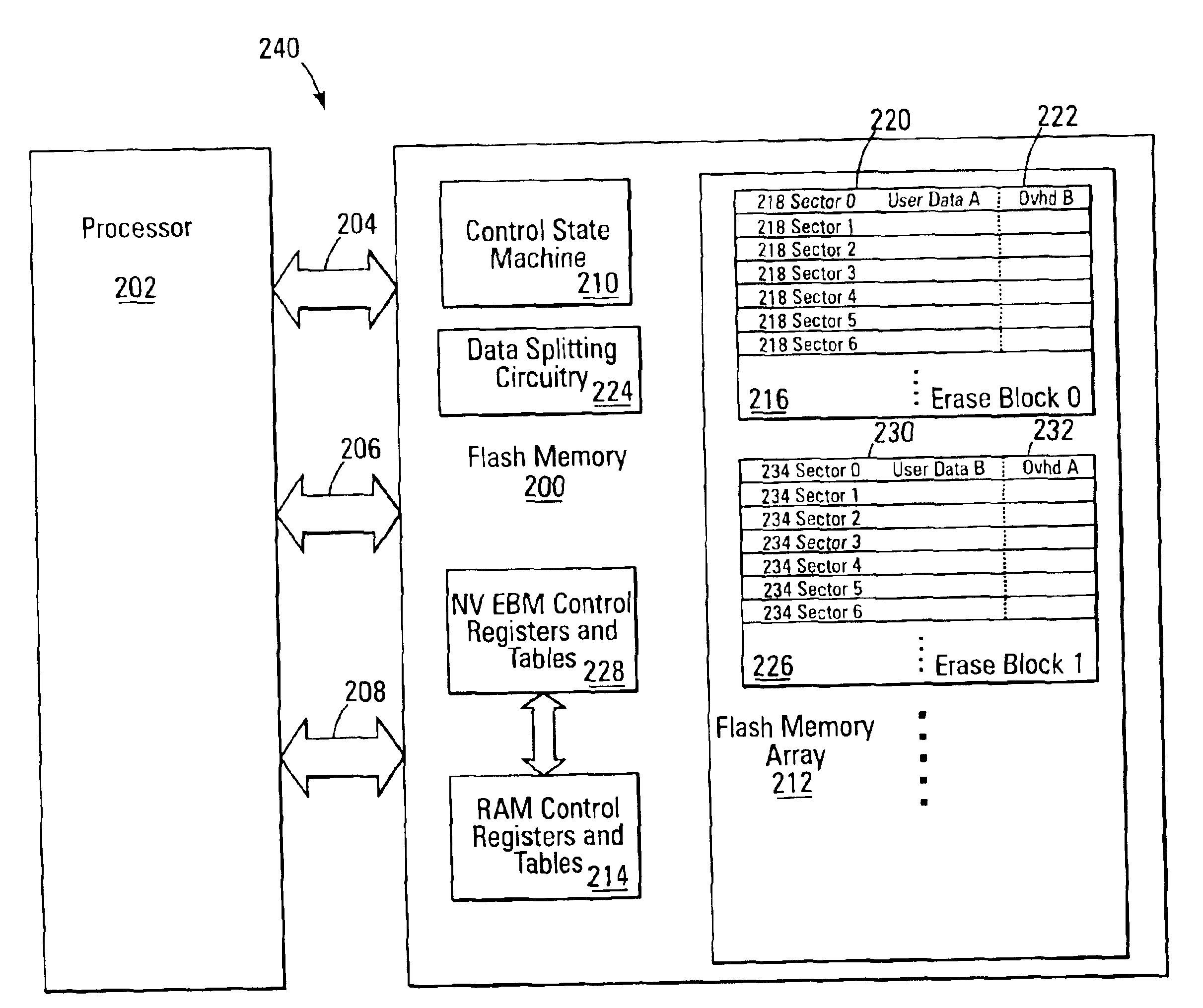
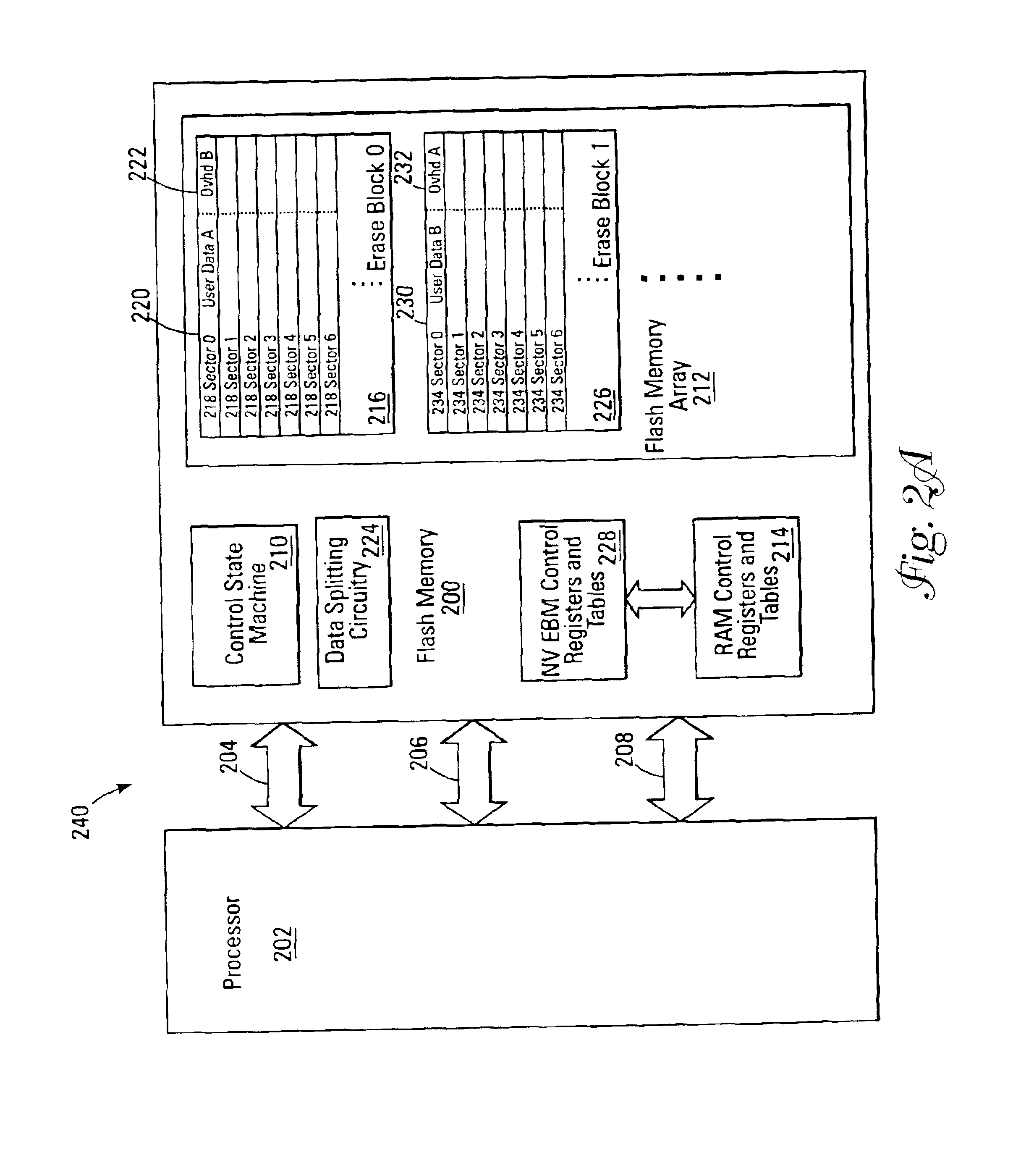
[0030]To improve data reliability in Flash memories, a Flash memory device, system, or data handling routine in accordance with an embodiment of the present invention splits the user data from the associated overhead data, storing each in...


PUM


Abstract

A Flash memory device, system, and data handling routine is detailed with a distributed erase block sector user / overhead data scheme that splits the user data and overhead data and stores them in differing associated erase blocks. The erase blocks of the Flash memory are arranged into associated erase block pairs in “super blocks” such that when user data is written to / read from the user data area of a sector of an erase block of the super block pair, the overhead data is written to / read from the overhead data area of a sector of the other associated erase block. This data splitting enhances fault tolerance and reliability of the Flash memory device.

Description

TECHNICAL FIELD OF THE INVENTION[0001]The present invention relates generally to integrated circuits and in particular the present invention relates to data management of Flash memory devices.BACKGROUND OF THE INVENTION[0002]Memory devices are typically provided as internal storage areas in the computer. The term memory identifies data storage that comes in the form of integrated circuit chips. There are several different types of memory used in modern electronics, one common type is RAM (random-access memory). RAM is characteristically found in use as main memory in a computer environment. RAM refers to read and write memory; that is, you can both write data into RAM and read data from RAM. This is in contrast to ROM, which permits you only to read data. Most RAM is volatile, which means that it requires a steady flow of electricity to maintain its contents. As soon as the power is turned off, whatever data was in RAM is lost.[0003]Computers almost always contain a small amount of ...

Claims


Application Information

Patent Timeline
Patent Type & Authority Patents(United States)
IPC IPC(8): G11C11/34G11C16/04G06F11/10
CPCG06F11/1068G06F11/1008G11C16/16
Inventor EGGLESTON, DAVIDMOSCHOPOULOS, ANTHONYMURRAY, MICHAELKEAYS, BRADY
Owner MICRON TECH INC
Why Eureka
Try Eureka