Chip stack with differing chip package types

a technology of chip packaging and chip stack, applied in the field of chip stacks, can solve the problems of inability to quickly, easily and inexpensively create chip stacks including dissimilar packaged chips, i.e., packaged chips of different types, and complex stacking process

Inactive Publication Date: 2005-06-21
M RED INC
View PDF21 Cites 80 Cited by
  • Summary
  • Abstract
  • Description
  • Claims
  • Application Information

AI Technical Summary

Problems solved by technology

Though bare dies or chips may also be used in the Z-Stacking process, such use tends to make the stacking process more complex and not well suited to automation.
However, one major drawback associated with current

Method used


Image

  • Chip stack with differing chip package types
  • Chip stack with differing chip package types
  • Chip stack with differing chip package types

Examples


Embodiment Construction

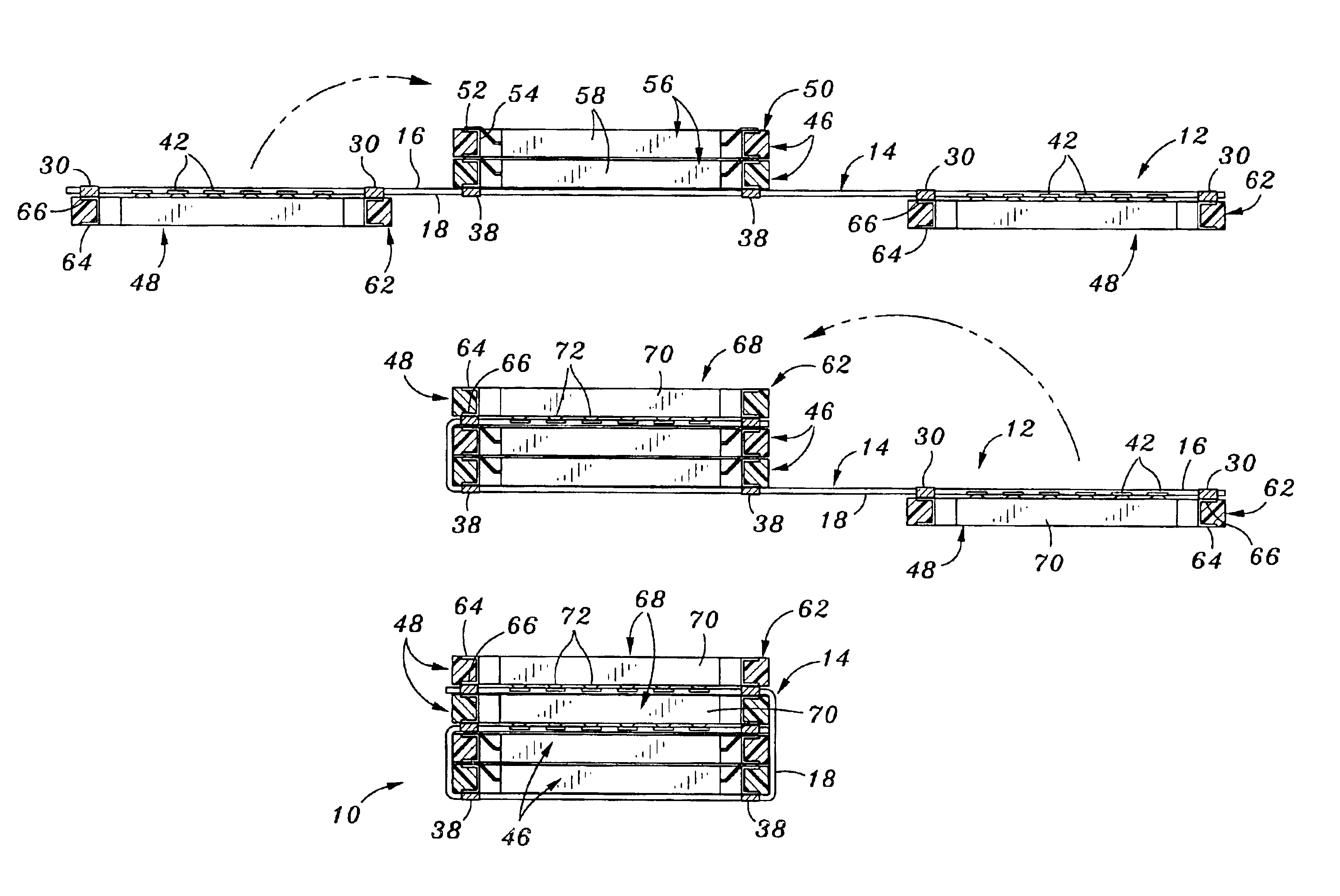
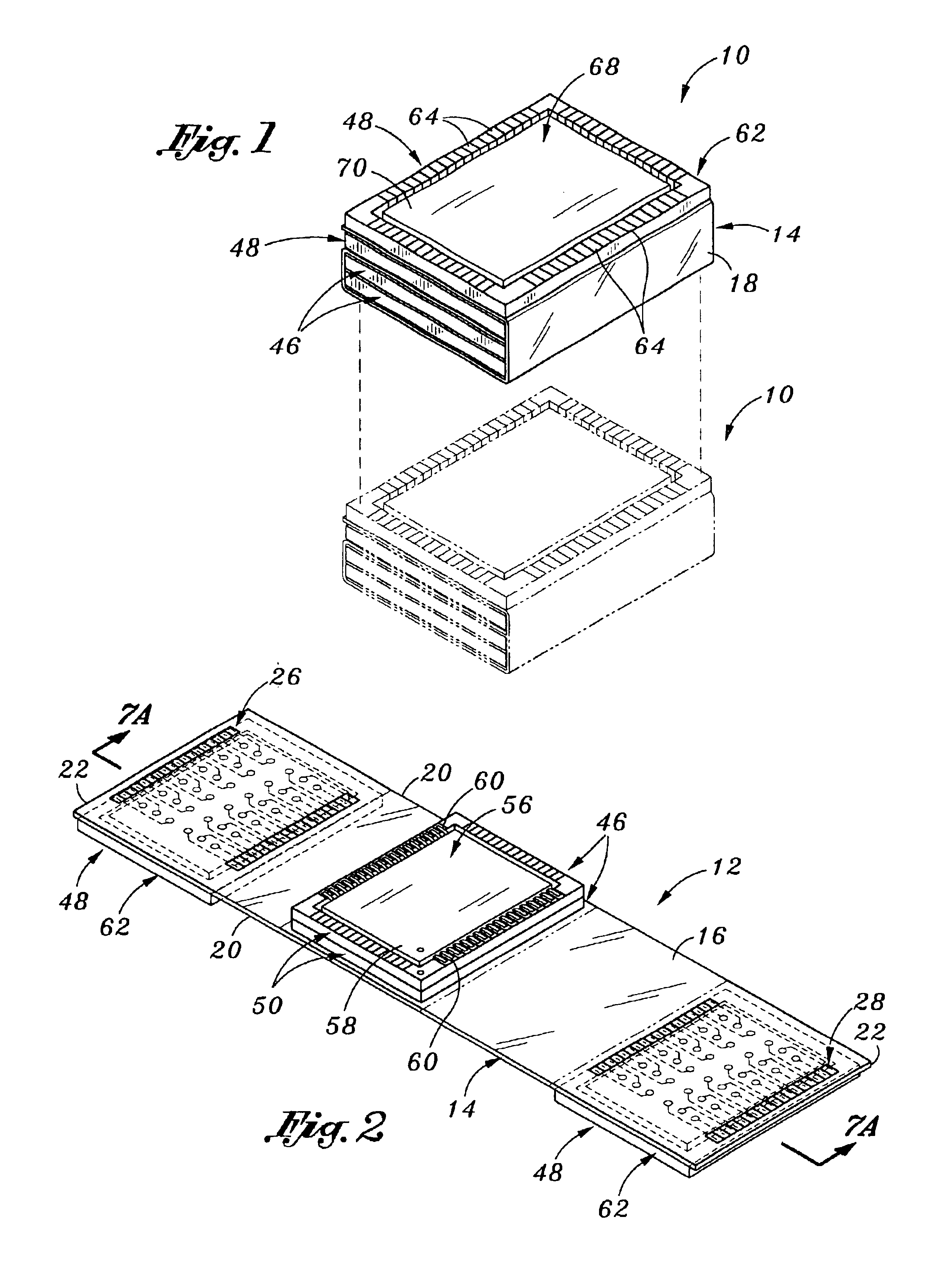
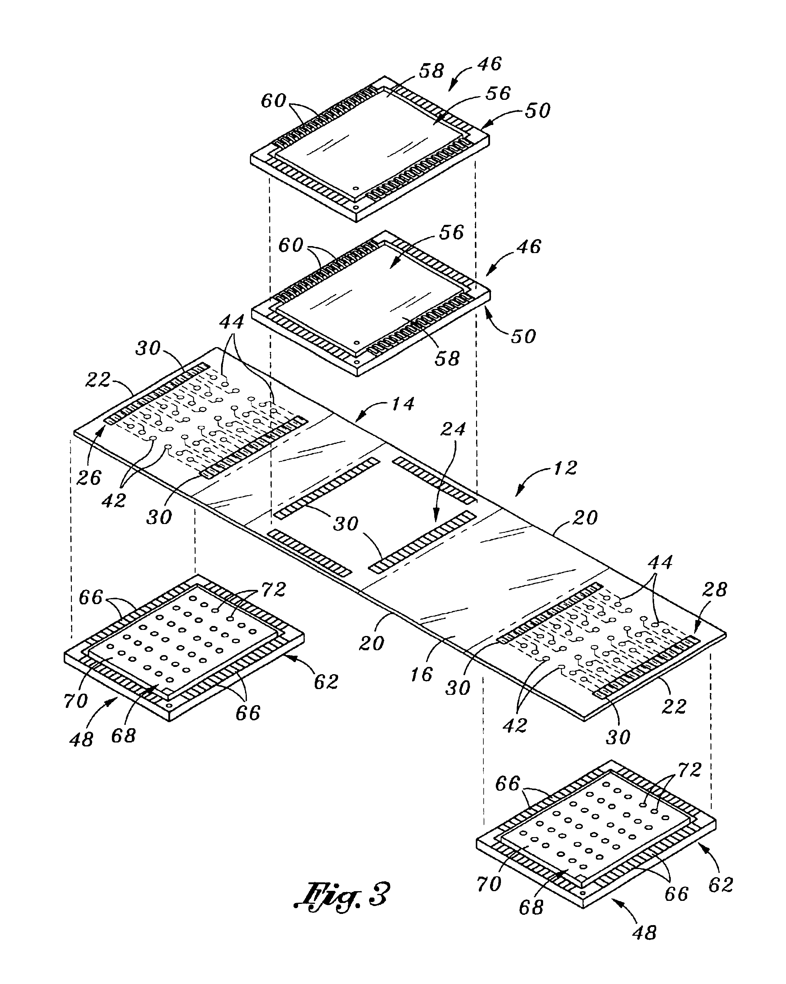
[0022]Referring now to the drawings wherein the showings are for purposes of illustrating a preferred embodiment of the present invention only, and not for purposes of limiting the same, FIG. 1 prospectively illustrates a chip stack 10 constructed in accordance with the present invention. As will be discussed in more detail below, the chip stack 10 is uniquely configured to allow dissimilar package chips or passive devices(e.g., TSOP devices and BGA devices) to be electrically connected to each other in stacked, vertical registry.

[0023]Referring now to FIGS. 2-4, the chip stack 10 comprises a flex circuit 12 which itself comprises a flexible substrate 14 having a generally planar top surface 16 (shown in FIGS. 2 and 3) and a generally planar bottom surface 18 (shown in FIG. 4). The substrate 14 preferably has a generally rectangular configuration and defines a pair of longitudinal peripheral edge segments 20 and a pair of lateral peripheral edge segments 22. The substrate 14 is pref...


PUM


Abstract

A chip stack comprising a flex circuit which itself comprises a flexible substrate having opposed, generally planar top and bottom surfaces. Disposed on the top surface of the substrate in spaced relation to each other are at least first and second top conductive patterns. Similarly, disposed on the bottom surface of the substrate in spaced relation to each other are at least first and second bottom conductive patterns. The first top and bottom conductive patterns are electrically connected to each other, as are the second top and bottom conductive patterns. At least one top chip package including a first packaged chip is electrically connected to the first top conductive pattern, with at least one bottom chip package including a second packaged chip being electrically connected to the second bottom conductive pattern. The substrate is folded such that the second top conductive pattern is electrically connected to the top chip package.

Description

CROSS-REFERENCE TO RELATED APPLICATIONS[0001]This is a division of U.S. application Ser. No. 09 / 912,010 filed Jul. 24, 2001 now U.S. Pat. No. 6,627,984.STATEMENT RE: FEDERALLY SPONSORED RESEARCH / DEVELOPMENT[0002](Not Applicable)BACKGROUND OF THE INVENTION[0003]The present invention relates generally to chip stacks, and more particularly to a chip stack including a uniquely configured flex circuit which allows different types of packaged chips to be placed into electrical communication with each other in a stacked configuration.[0004]Multiple techniques are currently employed in the prior art to increase memory capacity on a printed circuit board. Such techniques include the use of larger memory chips, if available, and increasing the size of the circuit board for purposes of allowing the same to accommodate more memory devices or chips. In another technique, vertical plug-in boards are used to increase the height of the circuit board to allow the same to accommodate additional memor...

Claims


Application Information

Patent Timeline
IPC IPC(8): H01L25/065H01L23/538H01L23/52
CPCH01L23/5387H01L25/0657H01L2225/06517H01L2225/06575H01L2225/06579H01L2924/0002H01L2924/3011H01L2924/00
Inventor BRUCE, TEDFORTHUN, JOHN A.
Owner M RED INC
Why Eureka
Try Eureka