Air channel interconnects for 3-d integration

a technology of air channel and integrated chips, which is applied in the direction of semiconductor devices, semiconductor/solid-state device details, electrical devices, etc., can solve the problems of not being able to solve the need for efficient heat removal through the 3-d device, the pressure to be delivered by the pumping system for the channel diameter is enormous and impractical, and the process is not practical for real-life chips. to achieve the effect of removing heat from the chip stack structur

Active Publication Date: 2011-02-10
GLOBALFOUNDRIES US INC
View PDF16 Cites 65 Cited by
  • Summary
  • Abstract
  • Description
  • Claims
  • Application Information

AI Technical Summary

Benefits of technology

[0017]In accordance with an exemplary embodiment of the present invention, a three-dimensional (3D) chip stack structure is provided. The 3D chip stack structure includes a plurality of vertically stacked chips which are interconnected and bonded together, wherein each of the vertically stacked chips includes one or more IC device strata. The 3D chip stack structure further includes an air channel interconnect network embedded within the chip stack structure. The air channel in

Problems solved by technology

However, thus far, there does not appear to be any effective and feasible way to resolve the need for efficient heat removal through the 3-D device.
However the following drawbacks may be associated with the above method such as: a complicated and inefficient structure wherein the fluid is fed either from top or bottom of the structure and through each of the layers, and therefore the vertical channel is just a hole similar to TSV for the fluid to feed through.
Also, the friction caused by the fluid flow through a channel increases the pressure required to maintain the fluid velocity by the square of the channel diameter, thereby necessitating an enormous and impractical amount of pressure to be delivered by a pumping system for channel diameters at these dimensions.
In addition, fluid cooling media may be susceptible to corrosion and contamination which may not make this process practical for the real-life chips.
Moreover, the above process may be an expensive process, wherein the micro-channels are formed after FEOL and BEOL with additional process steps wh

Method used


Image

  • Air channel interconnects for 3-d integration
  • Air channel interconnects for 3-d integration
  • Air channel interconnects for 3-d integration

Examples


Embodiment Construction

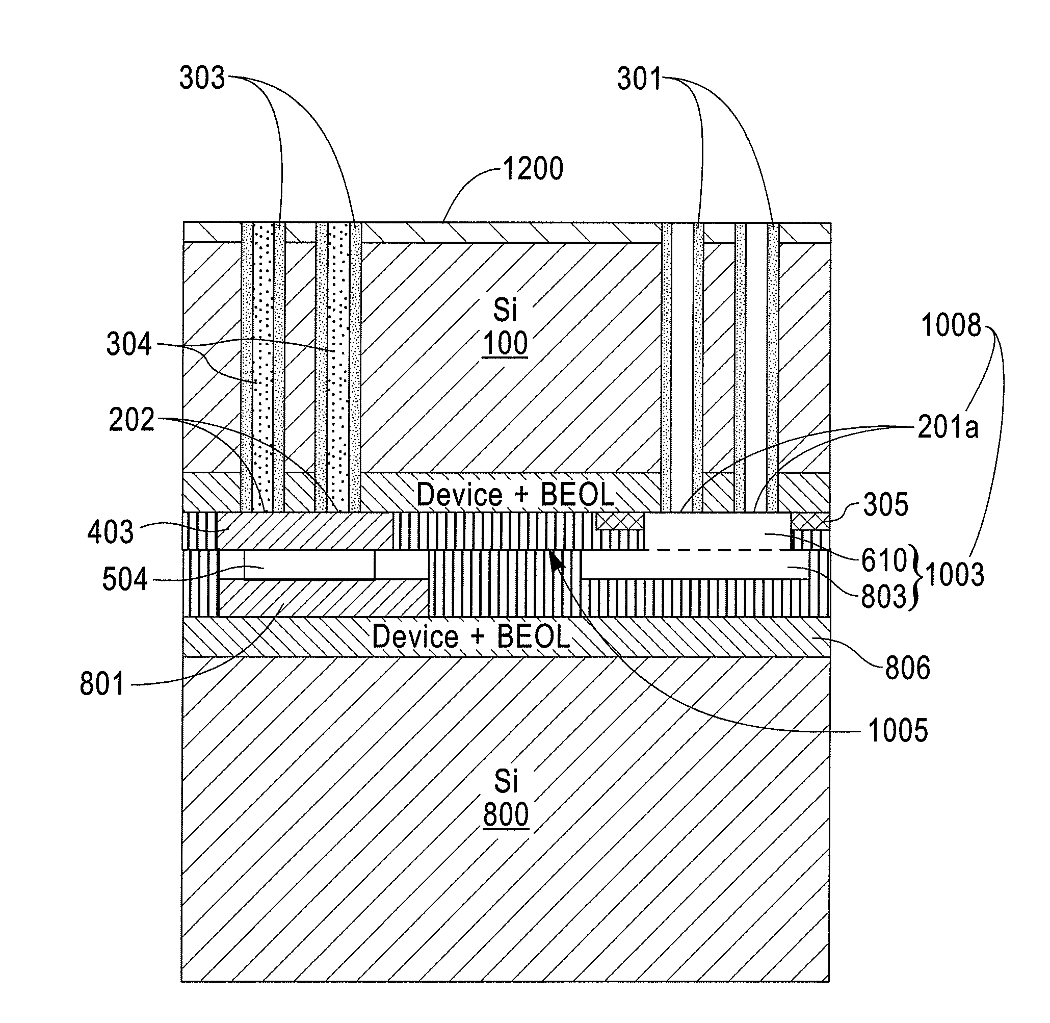
[0029]A three-dimensional wafer process integration in accordance with exemplary embodiments of the present invention includes an upper wafer process sequence, a lower wafer process sequence and wafer to wafer bonding sequence to form an air channel interconnect network within the upper wafer and the lower wafer and also in between the upper wafer and the lower wafer at a bonding interface thereof as illustrated in FIGS. 1-12 and described in detail below.

(1) Upper Wafer Processing Sequence:

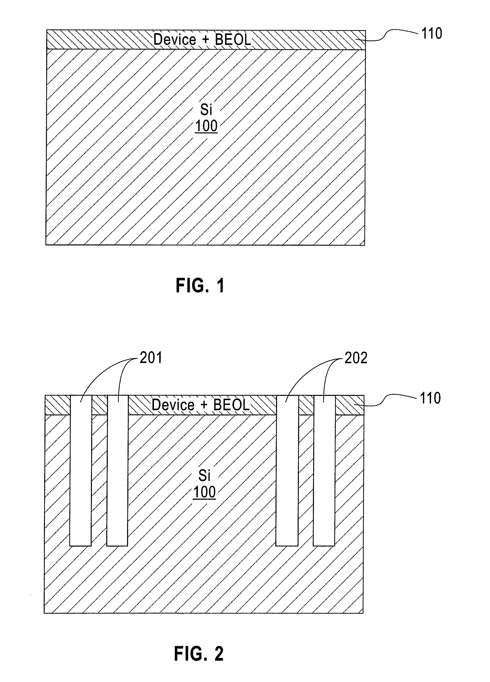
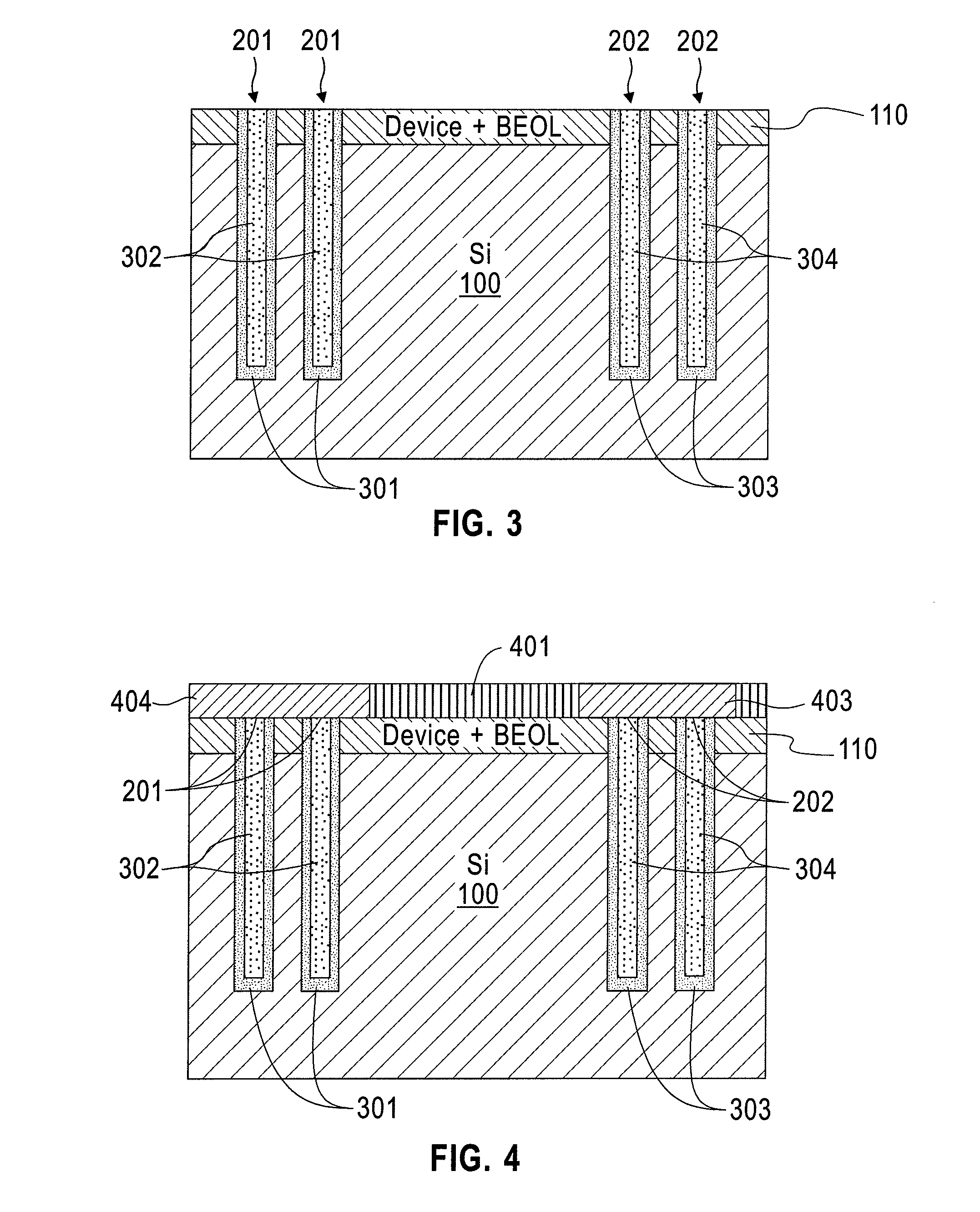
[0030]Referring to FIG. 1 an upper wafer 100, e.g., a silicon wafer, is processed through conventional front of line (FEOL) and back of line (BEOL) processes to have complementary metal oxide semiconductor (CMOS) devices (e.g. transistors, resistors and capacitors) and circuitry for connecting the CMOS devices provided in a device layer 110 which is formed of a dielectric material located on the front surface of the upper wafer 100.

[0031]Referring to FIG. 2, conventional lithography processing is...


PUM


Abstract

A three-dimensional (3D) chip stack structure and method of fabricating the structure thereof are provided. The 3D chip stack structure includes a plurality of vertically stacked chips which are interconnected and bonded together, wherein each of the vertically stacked chips include one or more IC device strata. The 3D chip stack structure further includes an air channel interconnect network embedded within the chip stack structure, and wherein the air channel interconnect network is formed in between at least two wafers bonded to each other of the vertically stacked wafers and in between at least two bonded wafers of the vertically stacked wafers at a bonding interface thereof. In addition, the 3D chip stack structure further includes one or more openings in a peripheral region of the chip stack structure that lead into and out of the air channel interconnect network, so that air can flow into and out of the air channel interconnect network through the one or more openings to remove heat from the chip stack structure.

Description

BACKGROUND[0001](i) Technical Field[0002]This invention relates to the manufacture of three-dimensional, vertical chip integration, and more particularly to methods for fabricating air channel interconnects for cooling.[0003](ii) Description of Related Art[0004]The trend in semiconductor integration is moving from two-dimensional (2-D) to three-dimensional (3-D) design. For example, to provide increased cache memory for microprocessors, a number of proposals are exploring methods for building three-dimensional (3-D) integrated circuits. A typical 3-D fabrication process includes building devices on wafers that are then thinned, providing vertical interconnections through the wafers, stacking the wafers so that vertical connections are established between wafers at different levels and bonding the wafers with a suitable material.[0005]As discussed below, there have been attempts to address certain difficulties associated with fabricating 3D integrated circuits including: (1) the need...

Claims


Application Information

Patent Timeline
IPC IPC(8): H01L23/532H01L21/50H01L21/768
CPCH01L21/76898H01L23/467H01L23/481H01L25/0657H01L25/50H01L2225/06513H01L2924/0002H01L2225/06541H01L2225/06589H01L2924/00H01L2224/16147H01L2224/16111H01L2224/13023H01L2224/13147H01L2224/80896H01L2224/81203H01L2924/00014
Inventor HSU, LOUIS L.JI, BRAIN L.LIU, FEIMURRAY, CONAL E.
Owner GLOBALFOUNDRIES US INC
Why Eureka
Try Eureka