Sensors based on giant planar hall effect in dilute magnetic semiconductors

a semiconductor and planar hall effect technology, applied in the field of sensors, can solve the problems of conflicting experimental results, complex electrical approach, and uncertainty in understanding the domain wall resistance, and achieve enhanced sensitivity, exceptional magnetic switching detection and analysis, and enhanced domain wall magnetic property measurement and analysis

Inactive Publication Date: 2005-06-28
CALIFORNIA INST OF TECH
View PDF11 Cites 15 Cited by
  • Summary
  • Abstract
  • Description
  • Claims
  • Application Information

AI Technical Summary

Benefits of technology

[0010]The present invention provides sensing systems and methods based on ferromagnetic semiconductor materials. The systems and methods of the present invention provide, inter alia, exceptional magnetic switching detection and analysis as well as enhanced domain wall magnetic property measurement and analysis relative to prior sensing systems. In one aspect, the present invention provides novel pressure sensors to detect pressure changes using magnetoresistive measurement techniques, and in particular GPHE techniques. In another aspect, the present invention provides magnetic switching detection sensors using ferromagnetic semiconductor-based materials that provide enhanced sensitivity relative to known materials and techniques. Such magnetic switching detection sensors according to the present invention are particularly useful as a read head sensor for HDD and other magnetic storage technologies.

Problems solved by technology

This is due to both the important role domain wall resistance might play in advanced spintronic devices, as well as the challenges it poses for both experimental and theoretical attempts to obtain fundamental understanding of its underlying physics.
However, this electrically-based approach is complicated by relatively small signal levels and the sample's multiple ferromagnetic layers.
At present, understanding of domain wall resistance is unsettled—there exists a conflicting body of work in the literature.
However, to date, experimental results that have emerged from these various methods are also conflicting; both positive (see, M. Viret, et al., Phys. Rev. Lett.
MR and GMR materials and devices however, are limited in sensitivity and therefore in application.

Method used


Image

  • Sensors based on giant planar hall effect in dilute magnetic semiconductors
  • Sensors based on giant planar hall effect in dilute magnetic semiconductors
  • Sensors based on giant planar hall effect in dilute magnetic semiconductors

Examples


Embodiment Construction

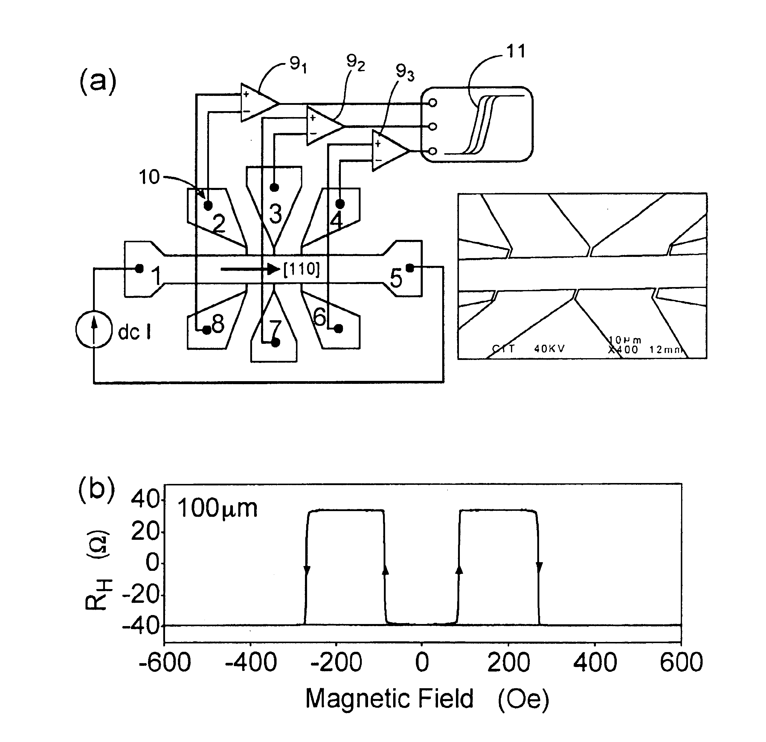
[0047]FIG. 1(a) shows a Hall device 10, including a measurement setup, according to an embodiment of the present invention. FIG. 1(a) also shows an electron micrograph of a typical Hall device 10. As shown, device 10 is arranged similar to a standard Hall bar having electrical contacts 1 and 5 positioned at opposite ends of the longitudinal axis (as shown, the [110] direction). Three pairs of transverse (Hall) voltage probes are provided. For example, probes 2 and 8 make up a pair, probes 3 and 7 make up another pair, and probes 4 and 6 make up the third pair. Although three sets of probes are shown, it is appreciated that two sets may be used or that more than three sets may be used in certain aspects.

[0048]Device 10 is preferably formed using a ferromagnetic based semiconductor material. In one embodiment, epilayers of (Ga, Mn)As are formed on a GaAs substrate and patterned to form the device. In one aspect, for example, device 10 is fabricated by growing a Ga1−xMnxAs epilayer, e....


PUM

PropertyMeasurementUnit
widthaaaaaaaaaa
widthsaaaaaaaaaa
widthsaaaaaaaaaa

Abstract

Ferromagnetic semiconductor-based sensor devices, including sensors for detecting pressure changes and sensors for detecting magnetic fields, such as switching events in a magnetic recording medium. The pressure sensors of the present invention detect pressure changes using magnetoresistive measurement techniques, and in particular GPHE techniques. Magnetic field detection sensors such as magnetic switching detection sensors include ferromagnetic semiconductor-based materials that provide enhanced sensitivity relative to known materials and techniques. Such magnetic switching detection sensors according to the present invention are particularly useful as a read head sensor for HDD and other magnetic storage technologies.

Description

CROSS-REFERENCES TO RELATED APPLICATIONS[0001]This application is a non-provisional application of, and claims priority to, U.S. Provisional Application Ser. Nos. 60 / 461,256, filed Apr. 8, 2003, 60 / 468,911, filed May 8, 2003, and 60 / 390,977, filed Jun. 21, 2002, the contents of which are hereby incorporated by reference in their entirety. This application is also related to U.S. Non-provisional application Ser. No. 10 / 602,537 filed on even date herewith, which is hereby incorporated by reference in its entirety.STATEMENT AS TO RIGHTS TO INVENTIONS MADE UNDER FEDERALLY SPONSORED RESEARCH OR DEVELOPMENT[0002]Not ApplicableBACKGROUND OF THE INVENTION[0003]The present invention relates generally to sensors, and more particularly to ferromagnetic semiconductor-based sensing devices and methods.[0004]Ferromagnetic semiconductors are of considerable current interest since they offer prospects for realizing semiconducting spintronics devices that have no analogs in a metallic ferromagnetic ...

Claims


Application Information

Patent Timeline
Patent Type & Authority Patents(United States)
IPC IPC(8): G01L9/16G01L9/00
CPCG01L9/16G01L9/0042
Inventor TANG, HONGXINGROUKES, MICHAEL L.
Owner CALIFORNIA INST OF TECH
Why Eureka
Try Eureka