

Apparatus for shear testing bonds on silicon substrate
a technology of silicon substrate and shear test, which is applied in the direction of material strength testing/measurement, semiconductor/solid-state device testing/measurement, instruments, etc., can solve the problems of increasing the cost of the apparatus, small components, and difficulty in forming bonds
- Summary
- Abstract
- Description
- Claims
- Application Information
AI Technical Summary
Benefits of technology
Problems solved by technology
Method used
Image

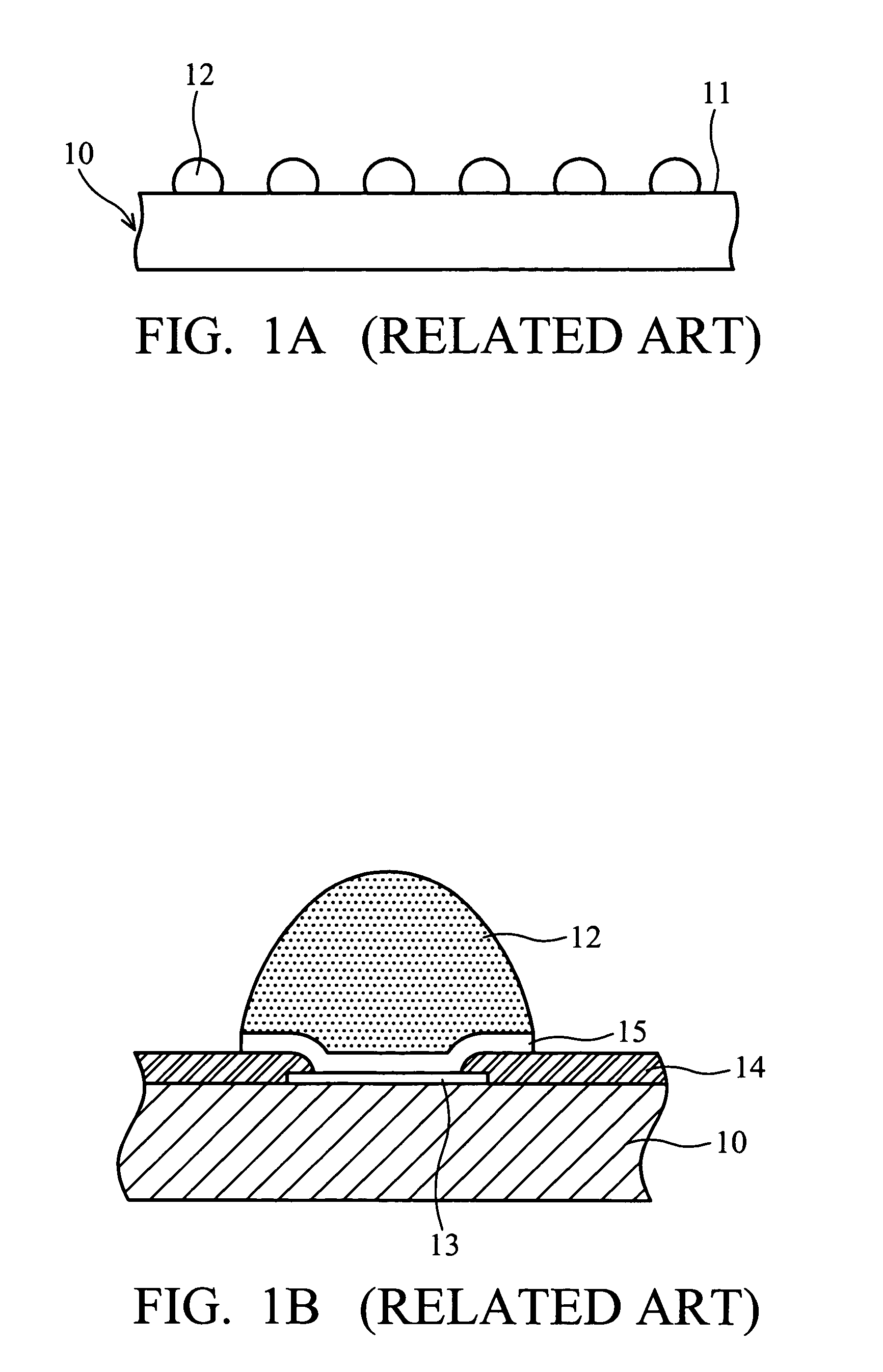
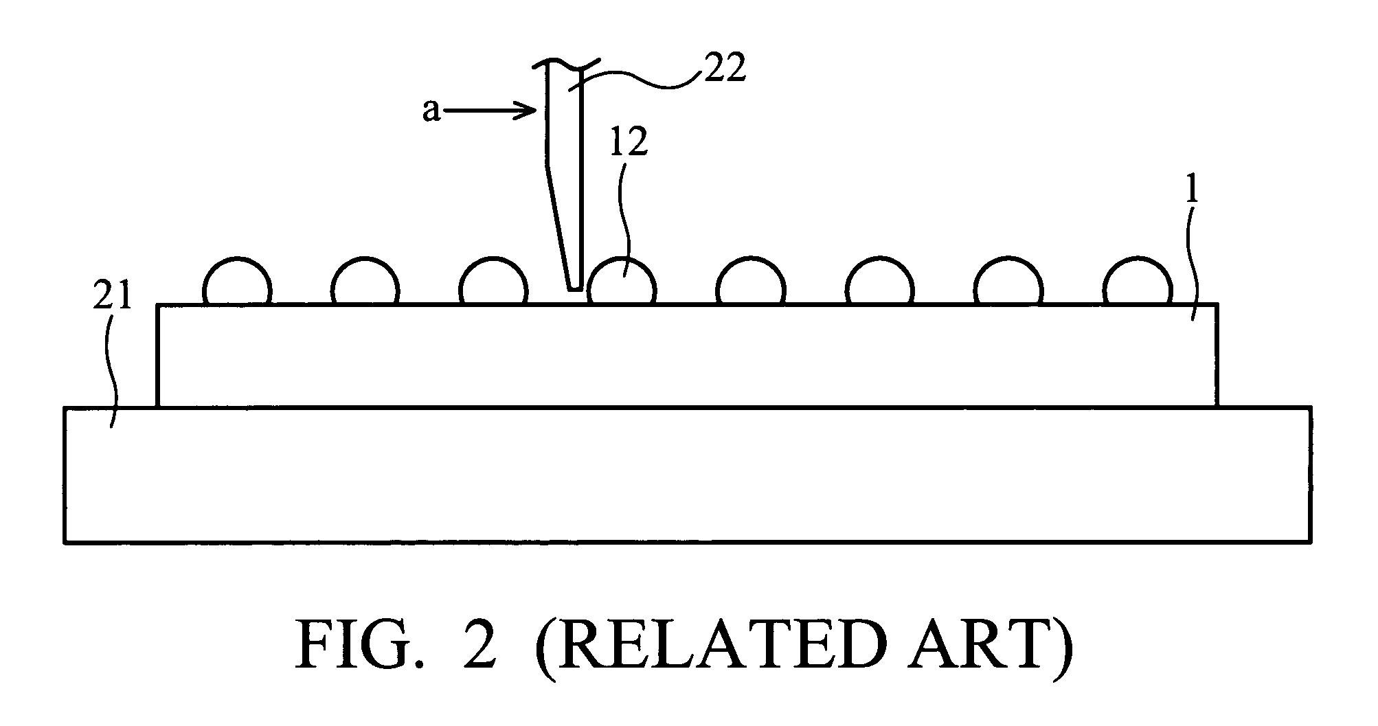
Examples
Embodiment Construction
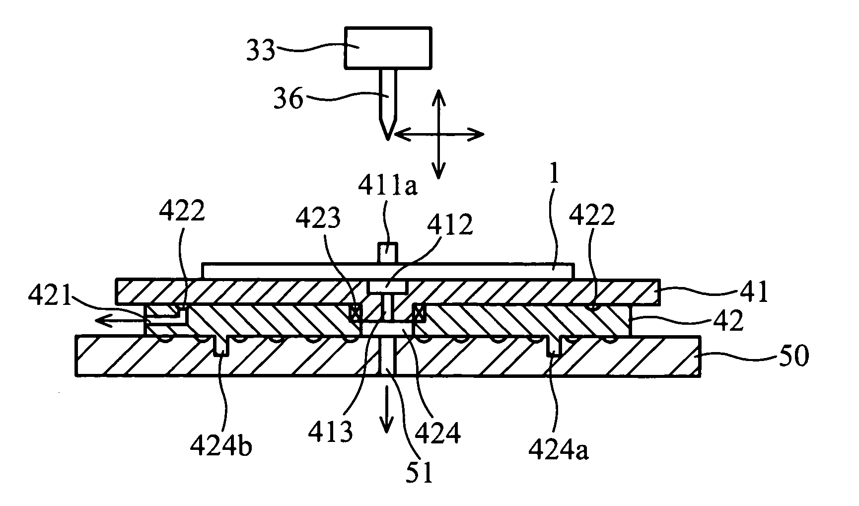
[0031]FIG. 3 is a block diagram of the shear testing apparatus of the invention. In FIG. 3, the shear testing apparatus 30 of the invention includes a vacuum chuck 50 connected to a vacuum pump 35 to fix a large-sized wafer, a probe 36 driven by a moving module 33, and a heating module 34 for heating the probe 36 to a required temperature to proceed with the shear test. A force sensor 32 consisting of the conventional strain gauges is applied to the probe 36 to measure the pulling shear force of the contact bump formed on the wafer. A control module 31 controls the moving module 33, the heating module 34 and the vacuum pump 35 and transforms the analog signal from the force sensor 32 into digital shear force data. Furthermore, the shear testing apparatus 30 also includes a removable platform 40 which can be assembled on the vacuum chuck 50 and connected to the vacuum pump 35 to fix a small-sized wafer, such that the shear testing apparatus 30 of the invention can test two different ...
PUM
| Property | Measurement | Unit |
|---|---|---|
| height | aaaaa | aaaaa |
| diameter | aaaaa | aaaaa |
| junction strength | aaaaa | aaaaa |
Abstract
Description
Claims
Application Information