Detecting over programmed memory

a detection and program technology, applied in the field of memory devices, can solve the problems of not checking to see, devices typically do not guarantee an upper limit on the threshold voltage, data being stored errors, etc., and achieve the effect of reducing the requirements of

Active Publication Date: 2005-07-12
SANDISK TECH LLC
View PDF33 Cites 310 Cited by
  • Summary
  • Abstract
  • Description
  • Claims
  • Application Information

AI Technical Summary

Benefits of technology

[0015]The present invention, roughly described, pertains to technology for detecting whether a memory device has been over programmed. Once it is detected that one or more memory devices have been over programmed, the system can remedy the situation by any one of a number of known means for correcting data. For example, the system can re-write the data to the same or a different memory device. Such over programming detection assures that the data is free from errors due to over programming so that the requirements of the ECC can be reduced.

Problems solved by technology

However, a problem arises when a number of the memory cells are to be programmed at the same time.
Faster programming of multiple memory cells can result in over-shooting desired threshold voltage level ranges, producing errors in the data being stored.
However, devices typically do not guarantee an upper limit on the threshold voltage.
Some devices do check to see if a soft programming process (described below) raised the threshold voltage too high; however, these devices do not check to see if a regular programming process raised the threshold voltage too high.
Over programming can cause the memory cell to store incorrect data, thereby, causing an error during subsequent read operations.
However, at least three problems arise when using ECC to correct errors due to over programming.
First, the ECC process requires a large amount of processing time and, therefore, considerably slows down the operation of the memory system.
Second, ECC requires additional dedicated hardware to perform the ECC in a reasonable amount of time.
Such dedicated hardware can take up a considerable amount of room on the memory system chips.
Third, if there are multiple errors, the ECC may not be able to correct the errors.

Method used


Image

  • Detecting over programmed memory
  • Detecting over programmed memory
  • Detecting over programmed memory

Examples


Embodiment Construction

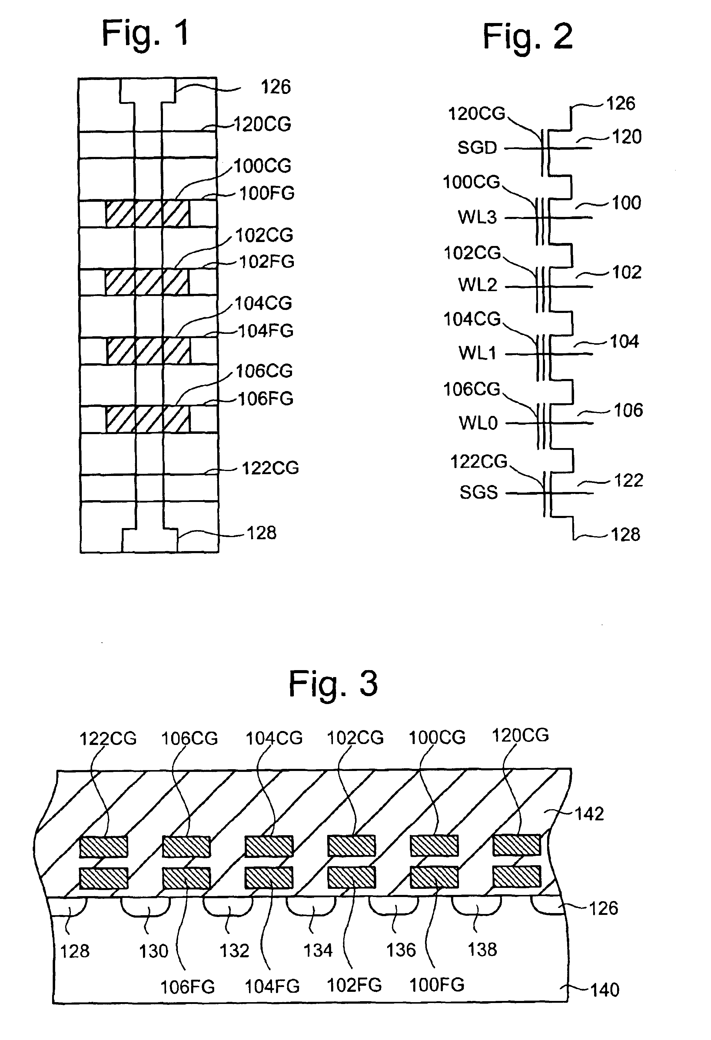
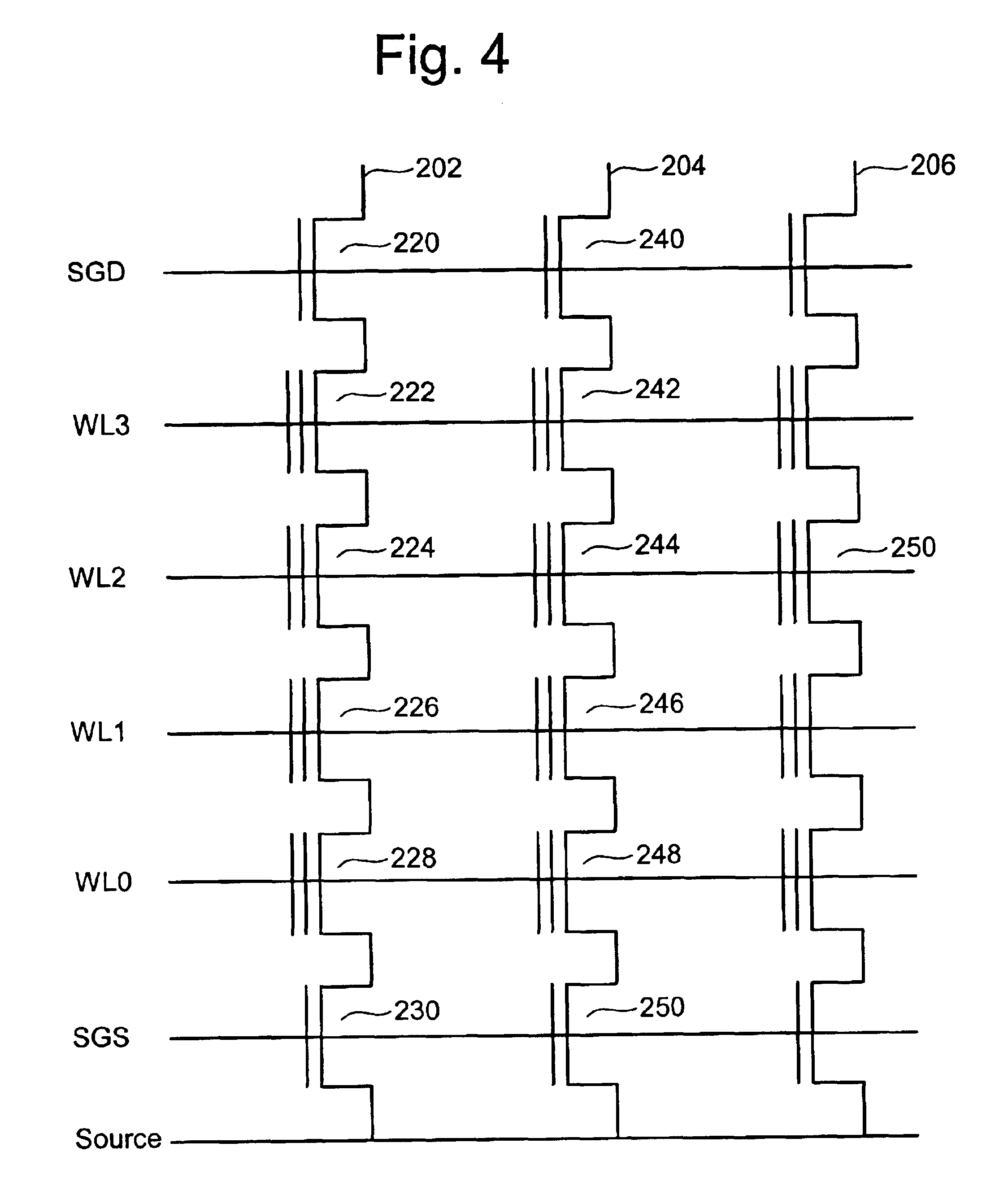
[0036]One example of a flash memory system uses the NAND structure, which includes arranging multiple transistors in series between two select gates. The transistors in series and the select gates are referred to as a NAND string. FIG. 1 is a top view showing one NAND string. FIG. 2 is an equivalent circuit thereof. The NAND string depicted in FIGS. 1 and 2 includes four transistors 100, 102, 104 and 106 in series and sandwiched between a first select gate 120 and a second select gate 122. Select gate 120 connects the NAND string to bit line 126. Select gate 122 connects the NAND string to source line 128. Select gate 120 is controlled by the applying appropriate voltages to control gate 120CG. Select gate 122 is controlled by applying the appropriate voltages to control gate 122CG. Each of the transistors 100, 102, 104 and 106 has a control gate and a floating gate. Transistor 100 has control gate 100CG and floating gate 100FG. Transistor 102 includes control gate 102CG and floatin...


PUM


Abstract

In a non-volatile semiconductor memory system (or other type of memory system), a memory cell is programmed by changing the threshold voltage of that memory cell. Because of variations in the programming speeds of different memory cells in the system, the possibility exists that some memory cells will be over programmed. That is, in one example, the threshold voltage will be moved past the intended value or range of values. The present invention includes determining whether the memory cells are over programmed.

Description

CROSS-REFERENCE TO RELATED APPLICATIONS[0001]This Application is related to U.S. patent application titled “DETECTING OVER PROGRAMMED MEMORY AFTER FURTHER PROGRAMMING,” by Jian Chen, Yan Li and Jeffrey W. Lutze, filed on the same day as the present application, which is incorporated herein by reference.BACKGROUND OF THE INVENTION[0002]1. Field of the Invention[0003]The present invention relates generally to technology for memory devices and, more specifically, to detecting whether memory devices have been over programmed.[0004]2. Description of the Related Art[0005]Semiconductor memory devices have become more popular for use in various electronic devices. For example, non-volatile semiconductor memory is used in cellular telephones, digital cameras, personal digital assistants, mobile computing devices, non-mobile computing devices and other devices. Electrical Erasable Programmable Read Only Memory (EEPROM) and flash memory are among the most popular non-volatile semiconductor mem...

Claims


Application Information

Patent Timeline
Patent Type & Authority Patents(United States)
IPC IPC(8): G11C11/56G11C16/04G11C16/34
CPCG11C11/5628G11C16/0483G11C16/3454G11C16/3459G11C16/3463G11C16/3418G11C16/34G11C11/56
Inventor CHEN, JIANLI, YANLUTZE, JEFFREY W.
Owner SANDISK TECH LLC
Why Eureka
Try Eureka