Heat releasing member, package for accommodating semiconductor element and semiconductor device

a technology for semiconductor elements and heat releasing components, which is applied in the direction of semiconductor devices, semiconductor/solid-state device details, electrical apparatus, etc., can solve the problems of increasing the thermal expansion coefficient between the semiconductor element and the heat releasing member cannot be joined firmly, and the heat emitted by the semiconductor element is becoming insufficient, etc., to achieve satisfactory dissipation of heat generated by the semiconductor element to the outside or the air, and high sealing reliability

Inactive Publication Date: 2005-07-26
KYOCERA CORP
View PDF4 Cites 30 Cited by
  • Summary
  • Abstract
  • Description
  • Claims
  • Application Information

AI Technical Summary

Benefits of technology

[0015]An object of the invention is to provide a heat releasing member that can dissipate heat emitted by a semiconductor element to the outside or the air satisfactorily and can adhere the semiconductor element to the heat releasing member firmly by using for a package for accommodating the semiconductor element, and provide a package for accommodating a semiconductor element using the heat releasing member and a semiconductor device using the same.
[0016]Another object of the invention is to provide a package for accommodating a semiconductor element that can dissipate heat generated in a semiconductor element satisfactorily to the outside or the air and in which the semiconductor element can be adhered firmly to the heat releasing member and high sealing reliability is provided by the sealing resin, and a semiconductor device using the same.

Problems solved by technology

However, the heat conductivity of the heat releasing member made of an alloy material of tungsten and copper or an alloy material of molybdenum and copper as described above is about 200 W / m·K, which is low for this requirement, and thus the heat releasing properties are becoming insufficient.
However, when the content of copper is increased in order to improve the heat conductivity, the difference in the thermal expansion coefficient between the semiconductor element and the heat release member is increased, so that the semiconductor element cannot be joined to the heat releasing member firmly.
Furthermore, in the package for accommodating a semiconductor element using a heat releasing member made of this composite material, copper expands and is plastically deformed at high temperatures when assembling the package, so that the heat releasing member does not return to the original state and the surface of the heat releasing member becomes rough.
However, in the package on which an insulating frame is attached so as to surround the mounting portion for a semiconductor element, the mounting portion cannot be polished.
However, when the surface roughness of the heat releasing member is significantly small, the area in which the heat releasing member and the sealing resin are in contact with each other is decreased, and the anchoring effect of the sealing resin to the heat releasing member is reduced, so that the bond strength between the heat releasing member and the sealing resin is degraded.
Thus, peeling may occur at the interface between the heat releasing member and the sealing resin.

Method used


Image

  • Heat releasing member, package for accommodating semiconductor element and semiconductor device
  • Heat releasing member, package for accommodating semiconductor element and semiconductor device
  • Heat releasing member, package for accommodating semiconductor element and semiconductor device

Examples


examples

[0195]Next, samples were produced in the following manner and the package for accommodating a semiconductor element and a semiconductor device of the invention was evaluated.

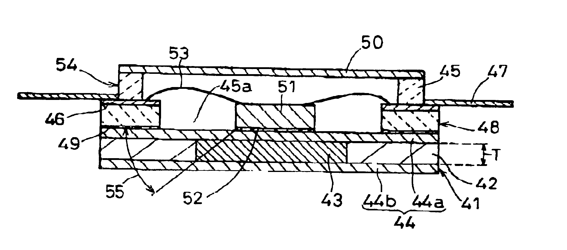
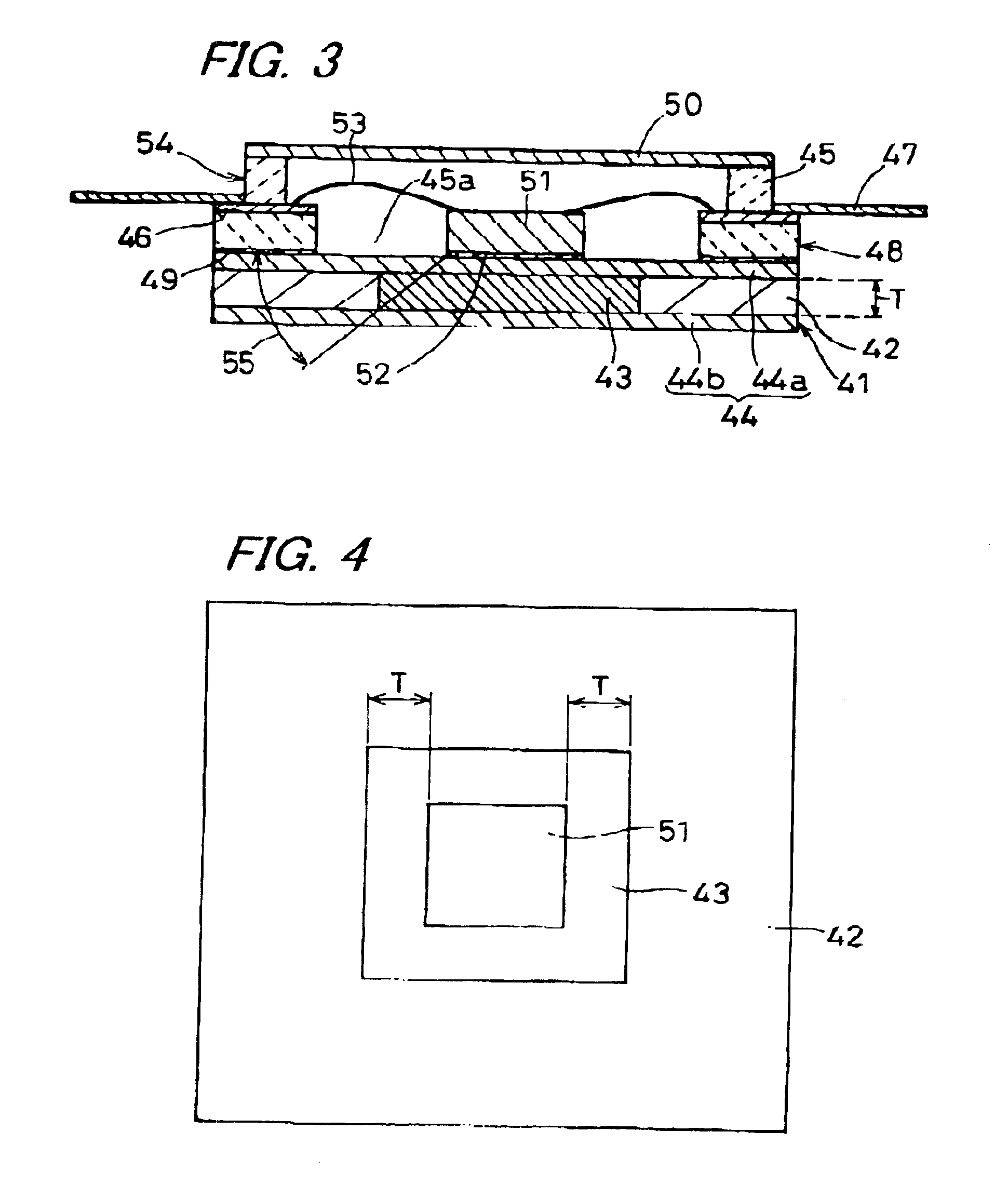
[0196]First, a releasing member having a size of 34 mm×17.4 mm, and a thickness of 1.9 mm was prepared as the heat releasing member 83 shown in FIG. 6.

[0197]The substrate 82 of the heat releasing member 83 is formed of a matrix material of tungsten and copper, and has a thickness of 1.52 mm. The thickness of the copper layers 86 (86a, 86b) of the heat releasing member 83 is each 0.19 mm.

[0198]The side surfaces of the copper layer 86a on the mounting portion side and the heat releasing member 83 are polished, and eighteen kinds of arithmetical mean roughness Ra from 0.01 μm to 36 μm respectively are prepared.

[0199]The insulating frame 81 formed of alumina ceramics was connected to the heat releasing member 83 with a Ag—Cu brazing material, and thus the package 88 for accommodating a semiconductor element was obta...


PUM


Abstract

A package for accommodating a semiconductor element includes a heat releasing member having a mounting portion for a semiconductor element, a frame having a wiring conductor, and a lid attached so as to cover the mounting portion. In the heat releasing member, a plurality of through-metal members made of a copper are buried in the mounting portion of a substrate made of a matrix of tungsten or molybdenum and copper to another surface. Copper layers are joined at least to upper and lower surfaces of a portion in which the through-metal members are buried, and a cross-section area of each of the through-metal members is gradually increased from the center side of the substrate to a joint portion with the copper layers.

Description

BACKGROUND OF THE INVENTION[0001]1. Field of the Invention[0002]The present invention relates to a package for accommodating a semiconductor element having a heat release structure with good heat releasing properties and a semiconductor device using the same. Furthermore, the present invention relates to a heat releasing member and a package for accommodating a semiconductor element having a heat release structure with good heat releasing properties, and a semiconductor device using the same.[0003]2. Description of the Related Art[0004]Conventionally, a semiconductor-element-accommodating package for accommodating a semiconductor element is generally formed of an insulating frame made of an electric insulating material such as aluminum oxide sintered substances, mullite sintered substances, or glass ceramic sintered substances, a heat releasing member on which a semiconductor element is mounted for satisfactorily releasing heat generated during operation thereof to the air and that ...

Claims


Application Information

Patent Timeline
Patent Type & Authority Patents(United States)
IPC IPC(8): H01L23/373H01L23/02H01L23/057H01L23/367H01L23/34H01L23/16H01L23/24
CPCH01L23/057H01L23/3677H01L23/3733H01L23/3735H01L23/24H01L2224/32188H01L2224/32225H01L2224/48091H01L2224/48227H01L2224/73265H01L2924/01012H01L2924/0102H01L2924/01025H01L2924/01046H01L2924/01078H01L2924/01079H01L2924/09701H01L2924/15153H01L2924/1517H01L2924/16195H01L2924/00014H01L24/48H01L2924/01019H01L2924/00H01L2924/181H01L2924/00012H01L2224/45099H01L2224/45015H01L2924/207
Inventor BASHO, YOSHIHIROMORI, RYUJIMIYAUCHI, MASAHIKO
Owner KYOCERA CORP
Why Eureka
Try Eureka