

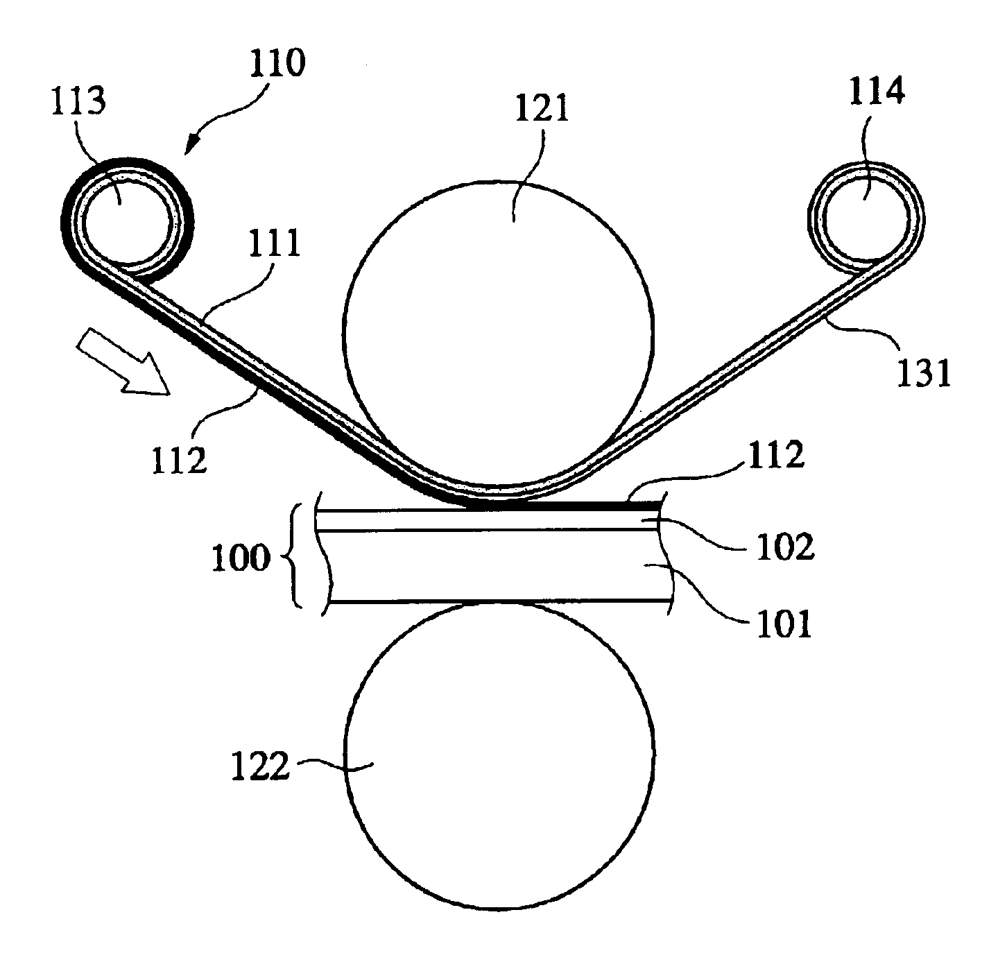
Method for producing organic electroluminescent device and transfer material used therein
a technology of electroluminescent devices and transfer materials, which is applied in the direction of diffusion transfer processes, instruments, other domestic objects, etc., can solve the problems of poor productivity, insufficient durability of organic light-emitting devices, and serious problems, and achieve good adhesion interface, good light-emitting efficiency, and low cost
- Summary
- Abstract
- Description
- Claims
- Application Information
AI Technical Summary
Benefits of technology
Problems solved by technology
Method used
Image

Examples
example 1
(A) Production of Transfer Material 1
[0119]Bar-coated onto one side of a 188-μm-thick temporary support made of polyether sulfone available from Sumitomo Bakelite Co., Ltd. was a coating solution 1 for a peeling layer having a composition of 30 parts by mass of a polyester resin HP320 having a glass transition temperature of 62° C. and a softening point of 95° C. available from Nippon Synthetic Chemical Industry Co., Ltd., 10 parts by mass of a silicone-modified acrylic resin solution US-3700 available from TOAGOSEI CO., LTD., 30 parts by mass of methyl ethyl ketone, and 30 parts by mass of toluene. The coated liquid was dried at 80° C. in vacuum for 2 hours to form the peeling layer in a thickness of 3.0 μm on the temporary support.
[0120]The maximum surface roughness Rmax of the resultant peeling layer was measured by an interatomic-force microscope method according to JIS B 0601-1982. Sampling was conducted in a lattice pattern at a pitch of 0.05 nm in an area of 20,000 nm×20,000 ...
example 2
[0129]A transfer material and an organic electroluminescent device were produced and evaluated in the same manner as in Example 1 except for using a coating solution 2 for a peeling layer having a composition of 18 parts by mass of a polyester resin HP301 having a glass transition temperature of 62° C. and a softening point of 105° C. available from The Nippon Synthetic Chemical Industry Co., Ltd., 2 parts by mass of silicone (Orgatics SI220 available from Matsumoto Trading Co., Ltd.) reacting with a peeling layer-forming resin, 40 parts by mass of methyl ethyl ketone, and 40 parts by mass of toluene, in place of the coating solution 1 for a peeling layer. The results are shown in Table 1.
example 3
[0130]A transfer material and an organic electroluminescent device were produced and evaluated in the same manner as in Example 1 except for using a coating solution 3 for a peeling layer having a composition of 17 parts by mass of a polyester resin HP320 having a glass transition temperature of 62° C. and a softening point of 95° C. available from The Nippon Synthetic Chemical Industry Co., Ltd., 3 parts by mass of silicone oil KF54 available from Shin-Etsu Chemical Co., Ltd., 40 parts by mass of methyl ethyl ketone, and 40 parts by mass of toluene, in place of the coating solution 1 for a peeling layer. The results are shown in Table 1.
PUM
| Property | Measurement | Unit |
|---|---|---|
| thickness | aaaaa | aaaaa |
| thickness | aaaaa | aaaaa |
| thickness | aaaaa | aaaaa |
Abstract
Description
Claims
Application Information