

Organic thin-film device and its production method
- Summary
- Abstract
- Description
- Claims
- Application Information
AI Technical Summary
Benefits of technology
Problems solved by technology
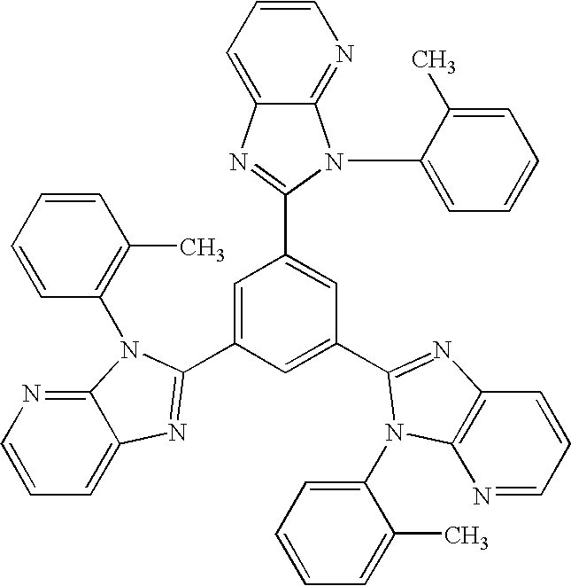
Method used
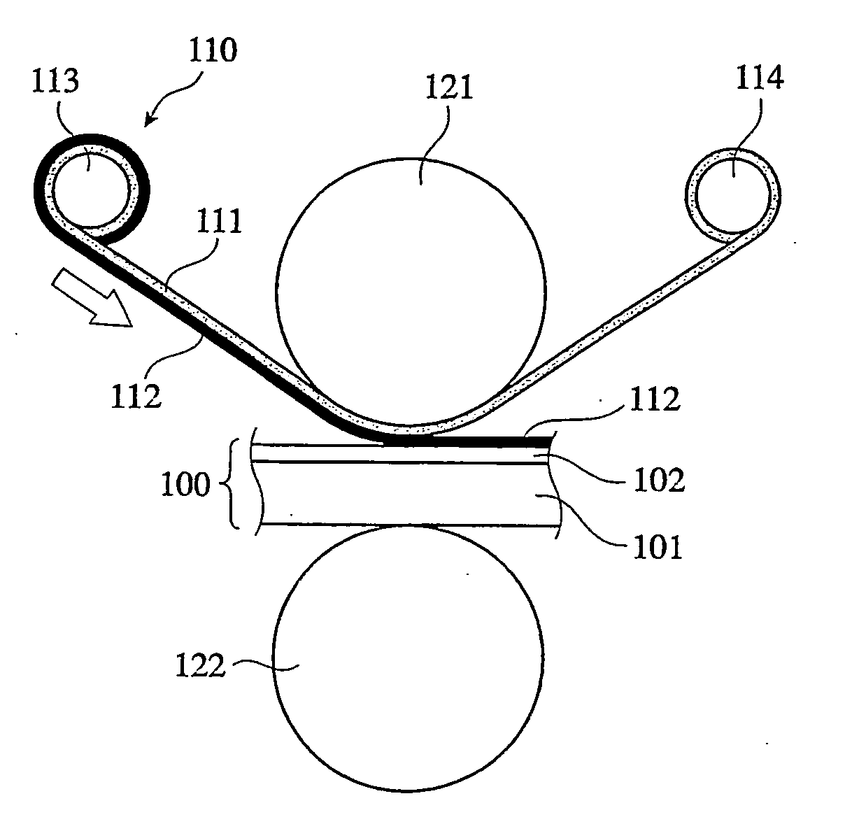
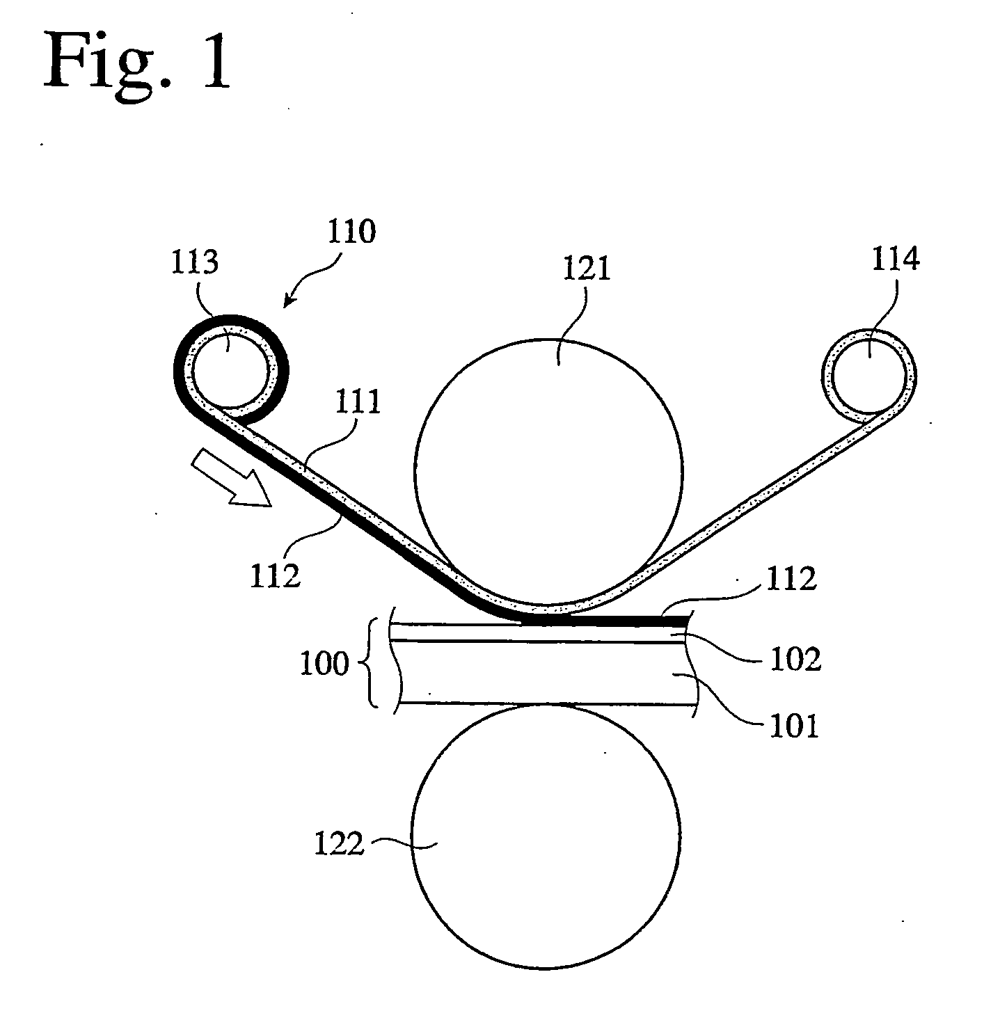
Image

Examples
examples 1 to 20
, COMPARATIVE EXAMPLES 1 TO 4
(A) Production of Laminate A
[0089] A glass plate of 0.5 mm×2.5 cm×2.5 cm was introduced into a washing vessel and washed with isopropyl alcohol (IPA), and then subjected to an oxygen plasma treatment. With a patterned vapor deposition mask having a light-emitting area of 5 mm×5 mm placed on one side of the oxygen plasma-treated glass plate, Al was vapor-deposited onto the glass plate in a reduced pressure atmosphere of about 0.1 mPa to form a 0.3-μn-thick electrode. Further as a dielectric layer, LiF was vapor-deposited onto the Al layer in a thickness of 3 nm in the same pattern as that of the Al layer. Aluminum lead wires were connected to Al electrodes to form Laminate A.
(B) Production of Laminate B
[0090] Laminate B was produced in the same manner as in Laminate A except for using a 50-μm-thick polyimide film (JPILEX-50S, available from Ube Industries, Ltd.) cut to 25 mm each in place of the glass plate.
(C) Production of Laminate C
[0091] A gla...
PUM
| Property | Measurement | Unit |
|---|---|---|
| Temperature coefficient of resistance | aaaaa | aaaaa |
| Efficiency | aaaaa | aaaaa |
| Efficiency | aaaaa | aaaaa |
Abstract
Description
Claims
Application Information