Supercharge Your Innovation With Domain-Expert AI Agents!

Semiconductor memory device capable of accessing data in continuous burst mode regardless of location of accessed data

a memory device and memory technology, applied in the field of semiconductor memory devices, can solve problems such as the performance limit of an overall system

Active Publication Date: 2005-08-16
SK HYNIX INC
View PDF12 Cites 2 Cited by
  • Summary
  • Abstract
  • Description
  • Claims
  • Application Information

AI Technical Summary

Benefits of technology

[0035]It is, therefore, a primary object of the present invention to provide a semiconductor memory device, in which a plurality of data is continuously inputted / outputted at a high speed regardless of locations of accessed data.

Problems solved by technology

However, since the conventional memory device cannot output consecutive data at a boundary portion between pages, it operates in the turned-off state of the wrap mode.
As a result, there is a limit to the performance of an overall system since an external device, such as a chipset, that transmits / receives to / from the memory device cannot always receive a plurality of data at a high speed.

Method used


Image

  • Semiconductor memory device capable of accessing data in continuous burst mode regardless of location of accessed data
  • Semiconductor memory device capable of accessing data in continuous burst mode regardless of location of accessed data
  • Semiconductor memory device capable of accessing data in continuous burst mode regardless of location of accessed data

Examples


Embodiment Construction

[0048]Hereinafter, the preferred embodiments of the present invention will be described in detail with reference to the accompanying drawings.

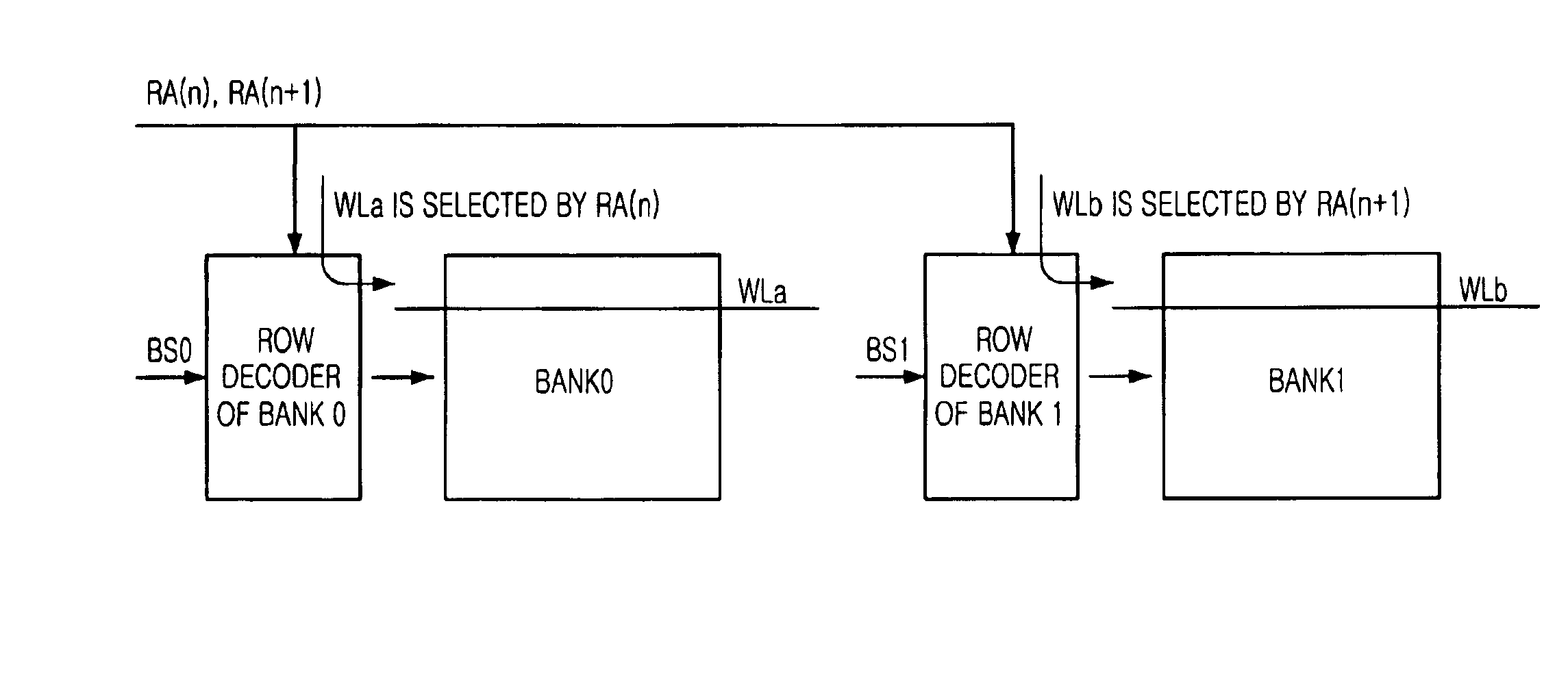
[0049]FIG. 4 is a block diagram of a memory device in accordance with a first preferred embodiment of the present invention.

[0050]Referring to FIG. 4, the memory device according to the present invention includes a bank 0 having a first word line WLa corresponding to a first row address RA(n), and a bank 1 having a second word line WLb corresponding to a second row address RA(n+1) that is consecutive to the first row address RA(n).

[0051]In accordance with an embodiment of the present invention, the memory device detects a location of a first data accessed corresponding to a first executing command in a burst mode in which N data stored corresponding to the consecutive addresses are accessed sequentially.

[0052]Then, considering the accessed first data and the number of data to be continuously outputted in the burst mode, it is determined whethe...


PUM


Abstract

There is provided a semiconductor memory device and a method for driving the same, which is capable of accessing data in a continuous burst mode regardless of locations of accessed data. The semiconductor memory device includes: a first bank including a first word line corresponding to a first row address; and a second bank including a second word line corresponding to a second row address, wherein the second row address is consecutive to the first row address. The method for driving a semiconductor memory device includes the steps of: receiving a first row address corresponding to a command; activating a word line of a first bank corresponding to the first row address; activating a word line of a second bank corresponding to a second row address, in which the second row address is consecutive to the first row address; sequentially accessing the predetermined number of data among the N data in a plurality of unit cells corresponding to the word line of the first bank; and sequentially accessing the remaining data in a plurality of unit cells corresponding to a word line of the second bank.

Description

FIELD OF THE INVENTION[0001]The present invention relates to a semiconductor memory device; and, more particularly, to a semiconductor memory device that is capable of accessing data in a continuous burst mode regardless of locations of accessed data.DESCRIPTION OF THE PRIOR ART[0002]A semiconductor memory device includes a plurality of banks in order to improve a system performance. A multi-memory bank structure makes it possible for each memory bank to independently access data and selects one of banks by decoding the most significant bit of a row address.[0003]FIG. 1 is a block diagram showing input / output (I / O) pins of a conventional memory device.[0004]Referring to FIG. 1, a conventional memory device includes a plurality of command input pins configured to receive command signals, n row address input pins RA0 to RAn−1 configured to receive n row addresses, m column address input pins CA0 to CAm−1 configured to receive m column addresses, and a plurality of data I / O pins DQ0 to...

Claims


Application Information

Patent Timeline
IPC IPC(8): G11C7/10G11C8/00G11C8/12G11C8/08
CPCG11C7/1018G11C8/08
Inventor AHN, JIN-HONGHONG, SANG-HOONKO, JAE-BUMKIM, SE-JUN
Owner SK HYNIX INC
Features
  • R&D
  • Intellectual Property
  • Life Sciences
  • Materials
  • Tech Scout
  • Unparalleled Data Quality
  • Higher Quality Content
  • 60% Fewer Hallucinations
Learn More