Memory device and method having low-power, high write latency mode and high-power, low write latency mode and/or independently selectable write latency

a memory device and memory technology, applied in the field of dynamic random access memories, can solve the problems of increasing the power consumption of memory devices in portable personal computers, affecting the length of time they can be used, and the power consumption of memory devices can be important, so as to minimize increase the write latency of memory devices, and avoid increased write latencies

Inactive Publication Date: 2005-08-23
ROUND ROCK RES LLC
View PDF18 Cites 53 Cited by
  • Summary
  • Abstract
  • Description
  • Claims
  • Application Information

AI Technical Summary

Benefits of technology

[0010]A method and circuit for a memory device allows the memory device to operate in either a low-power mode that may increase the write latency of the memory device or a high-power mode that minimizes the write latency of the memory device. In the low-power mode, the memory device operates in the conventional fashion described above to remove power to the write receivers in the memory device except when the memory device detects a write access to that memory device. In the high-power mode, power is not removed from the write receivers under most circumstances so the write receivers can immediately couple write data to internal circuitry, thereby avoiding increased write latencies that may occur when operating in the low-power mode. However, even in the high-power mode, power is preferably removed from the write receivers when none of the rows of memory cells in the memory device is active. Power is also preferably removed from the write receivers even in the high-power mode when the read transmitters in the memory device are active. The method and circuit for allowing memory devices to operate in either a low-power mode or a high-power mode is preferably used in dynamic random access memory (“DRAM”) devices, and such DRAM devices may be used in a computer system or some other electronic system.

Problems solved by technology

For example, the power consumed by memory devices used in portable personal computers greatly affects the length of time they can be used without the need to recharge batteries powering such computers.
Power consumption can also be important even where memory devices are not powered by batteries because it may be necessary to limit the heat generated by the memory devices.
In general, memory device power consumption increases with both the capacity and the operating speed of the memory devices.
As the speed of memory devices increases, the large number of signal lines in the memory devices change state more rapidly, consuming power with each state change.
Each time a data bit or address bit coupled to one of these receivers changes state, the receivers switch, thereby consuming power.
The power consumed by switching the receivers in all of the other memory device thus constitutes wasted power.
Although power can be removed from the data receivers and transmitters when a memory device is inactive, power cannot similarly be removed from command and address receivers because they must be active to detect when a read or a write access is directed to that memory device.
If power were removed from the command and address buffers, they would be unable to couple the command and address signals to internal circuitry that detects a read or a write access directed to that memory device.
Latencies of this magnitude can greatly slow the operating speed of conventional memory devices.
Thus, the problem of increased latencies caused by selectively removing power to receivers or transmitters exists only for removing power to write receivers.

Method used


Image

  • Memory device and method having low-power, high write latency mode and high-power, low write latency mode and/or independently selectable write latency
  • Memory device and method having low-power, high write latency mode and high-power, low write latency mode and/or independently selectable write latency
  • Memory device and method having low-power, high write latency mode and high-power, low write latency mode and/or independently selectable write latency

Examples


Embodiment Construction

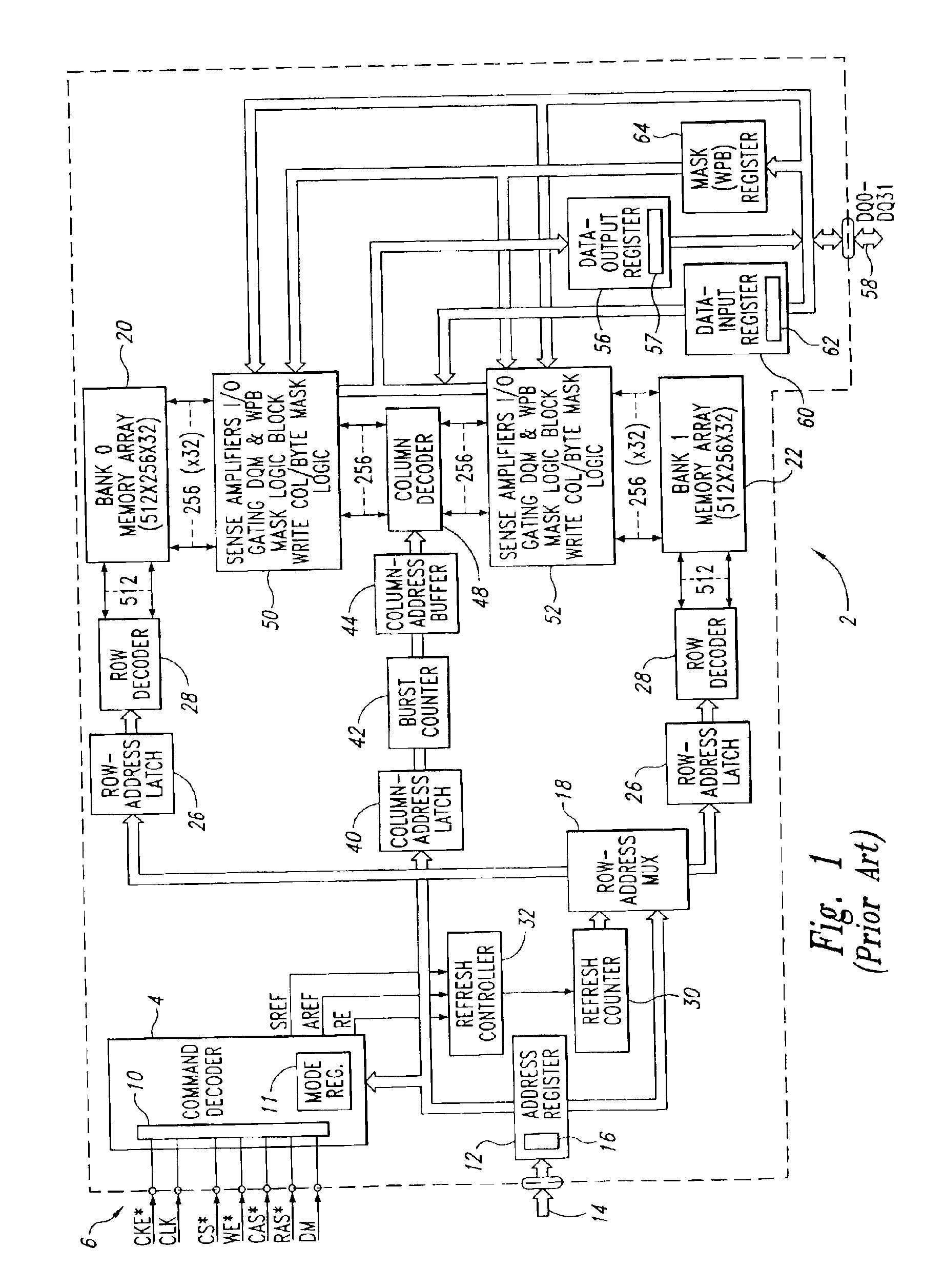
[0014]FIG. 1 is a block diagram of a conventional synchronous dynamic random access memory (“SDRAM”) 2 that can utilize a dual-power system according to one embodiment of the invention. However, it will be understood that various embodiments of the present invention can also be used in other types of DRAMs or other types of memory devices.

[0015]The operation of the SDRAM 2 is controlled by a command decoder 4 responsive to high-level command signals received on a control bus 6. These high level command signals, which are typically generated by a memory controller (not shown in FIG. 1), are a clock enable signal CKE*, a clock signal CLK, a chip select signal CS*, a write enable signal WE*, a row address strobe signal RAS*, a column address strobe signal CAS*, and a data mask signal DM, in which the “*” designates the signal as active low. The command decoder 4 includes a plurality of input buffers or command receivers, collectively designated by reference numeral 10, through which th...


PUM


Abstract

A logic circuit operates write receivers in a dynamic random access memory device in either a low-power mode, high write latency mode or a high-power mode, low write latency mode. The logic circuit receives a first signal indicative of whether the high-power, low write latency mode has been enabled, a second signal indicative of whether a row of memory cells in the memory device is active, a third signal indicative of whether the memory device is being operated in a power down mode, and a fourth signal indicative of whether read transmitters in the memory device are active. The logic circuit maintains power to the write receivers whenever the high-power, low write latency mode has been enabled if a row of memory cells in the memory device is active, the memory device is not being operated in the power down mode, and the read transmitters in the memory device are not active.

Description

TECHNICAL FIELD[0001]This invention relates to dynamic random access memories (“DRAMs”), and, more particularly, to a circuit and method for operating DRAMs in either a low-power, high write latency mode or a high-power, low write latency mode.BACKGROUND OF THE INVENTION[0002]The power consumed by integrated circuits can be a critical factor in their utility in certain applications. For example, the power consumed by memory devices used in portable personal computers greatly affects the length of time they can be used without the need to recharge batteries powering such computers. Power consumption can also be important even where memory devices are not powered by batteries because it may be necessary to limit the heat generated by the memory devices.[0003]In general, memory device power consumption increases with both the capacity and the operating speed of the memory devices. As the capacity of memory devices increase, for example, the memory devices contain more memory cells that...

Claims


Application Information

Patent Timeline
Patent Type & Authority Patents(United States)
IPC IPC(8): G11C7/10
CPCG11C7/1045G11C7/1078G11C7/1087G11C7/1096G11C7/22G11C11/4074G11C11/4076G11C11/4093G11C2207/2227G11C5/14
Inventor JOHNSON, CHRISTOPHER S.JOHNSON, BRIAN
Owner ROUND ROCK RES LLC
Why Eureka
Try Eureka